Project story, Instruments and Skills

Detailed fabrication journeys and behind-the-scenes engineering

Nanomechanical Gas Sensor: Concept to Cleanroom Fabrication, Process Development, Optimization and Troubleshooting Geometrical Structures

Jump to published articles of this project

Following my Ph.D. at Shizuoka University—where my focus was on MWCNT-based flexible pressure sensors—I transitioned into the microfabrication cleanroom environment at Tohoku University. Entering the lab of the highly esteemed Prof. Takahito Ono, I was tasked with leading a high-stakes, industry-funded project with Mitsui Chemicals. The objective was clear but challenging: develop, optimize, and scale the fabrication process for a novel Nanomechanical Gas Sensor intended for high-volume commercialization.

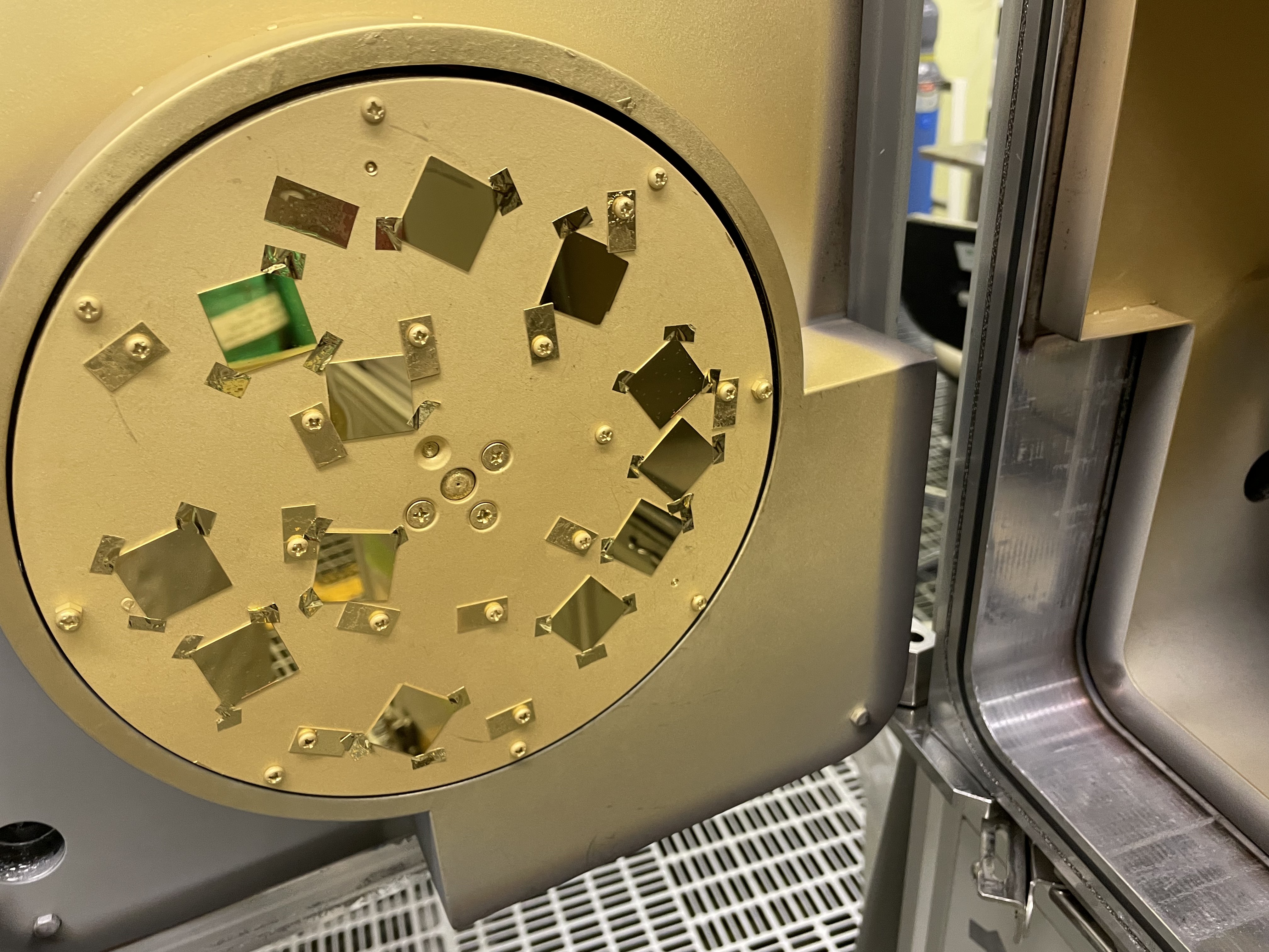
The core sensing mechanism relied on an ultra-sensitive micro-electromechanical systems (MEMS) architecture. Previous researchers had struggled to empirically prove the sensing principle due to fabrication yield and integration challenges. Recognizing the critical need for process control, I initiated a rigorous technical deep-dive, undergoing comprehensive training on Class-100 cleanroom equipment to master the metrology, lithography, and etching systems required for device realization.

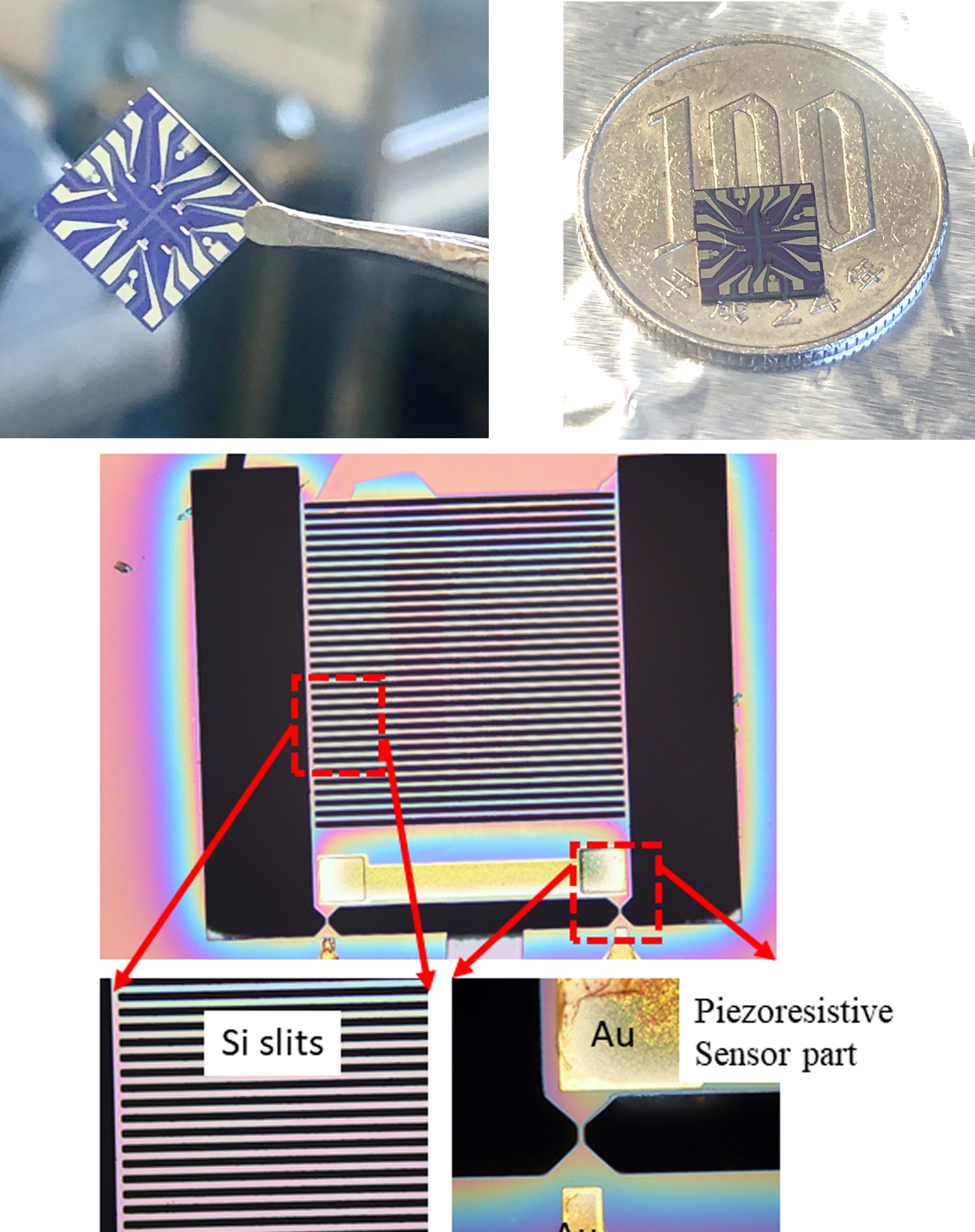
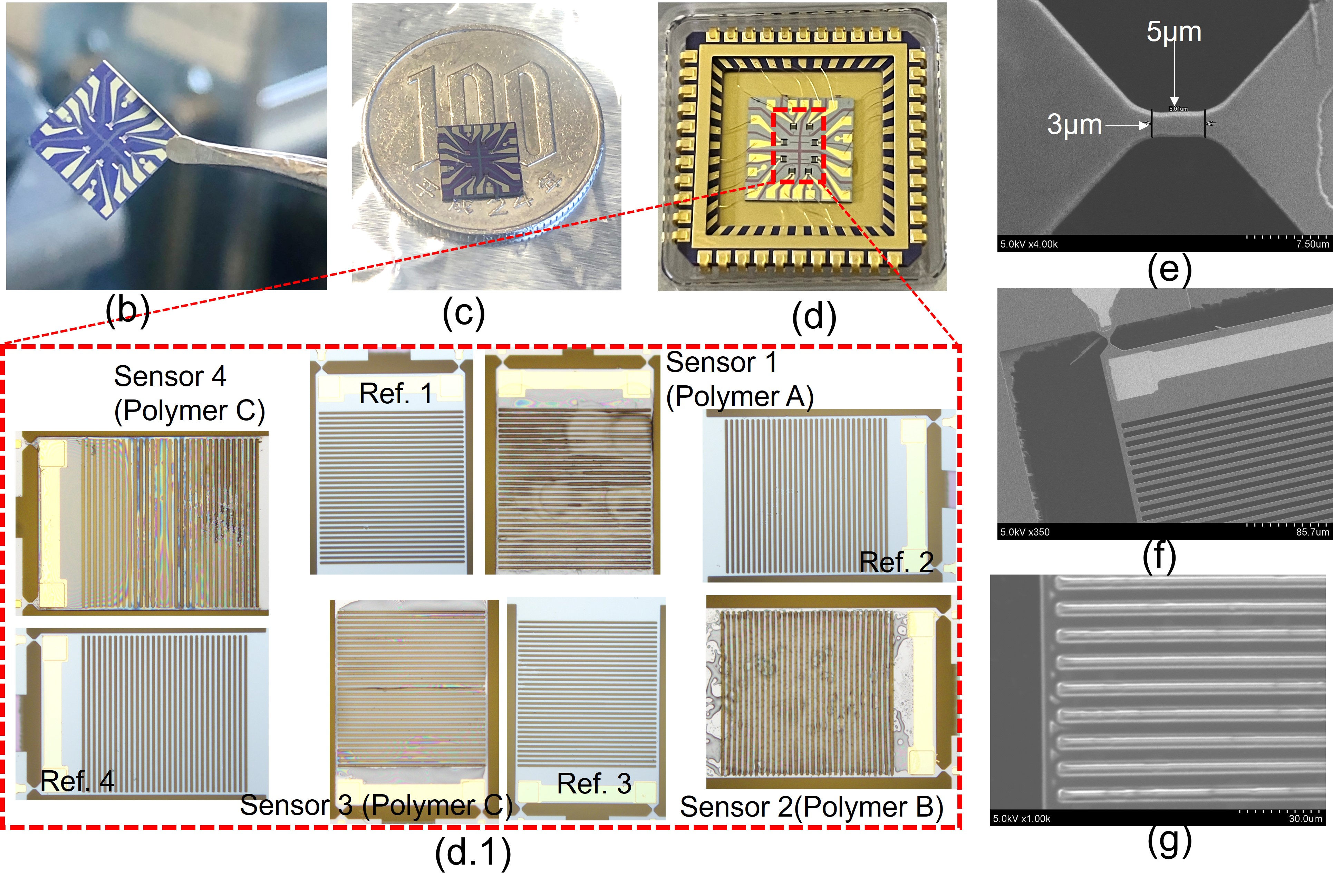
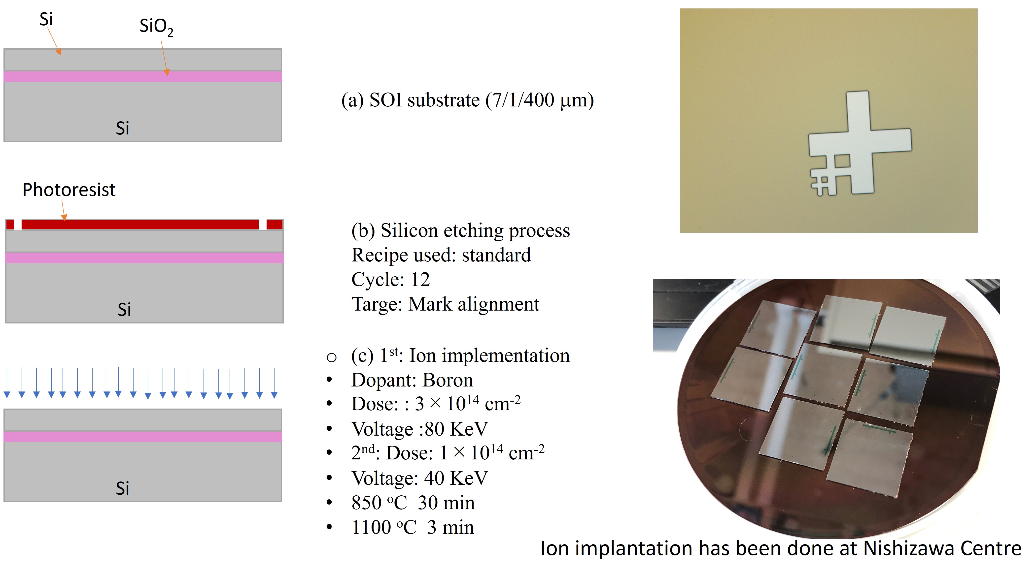
The finalized chip architecture consisted of 8 identical sensing arrays. Each array featured 20 suspended Silicon slits, precisely engineered over two 3 to 5-micrometer piezoresistive transduction elements. To ensure structural integrity and electrical isolation, I selected a Silicon-on-Insulator (SOI) wafer as the foundational substrate. The SOI structure—comprising a 5-7 μm top device layer, a SiO2 buried oxide (BOX) isolation layer, and a robust handle layer—provided the optimal mechanical foundation for releasing the suspended nanostructures while minimizing parasitic signal loss.

The Cleanroom Journey & Instrumentation

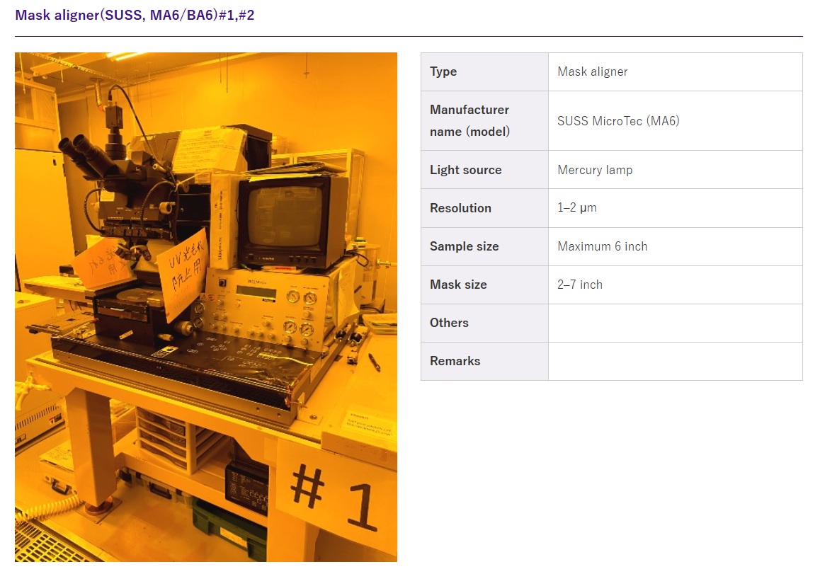
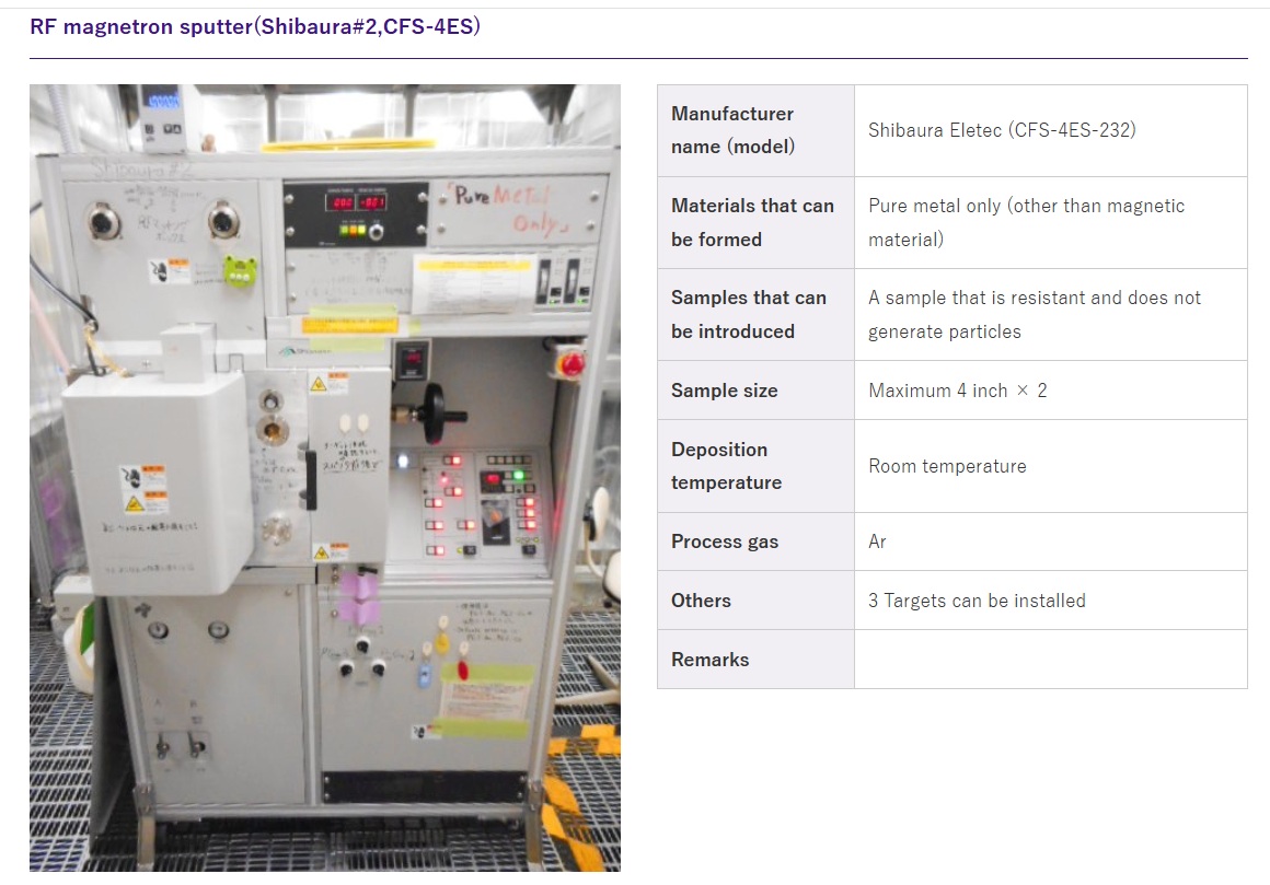
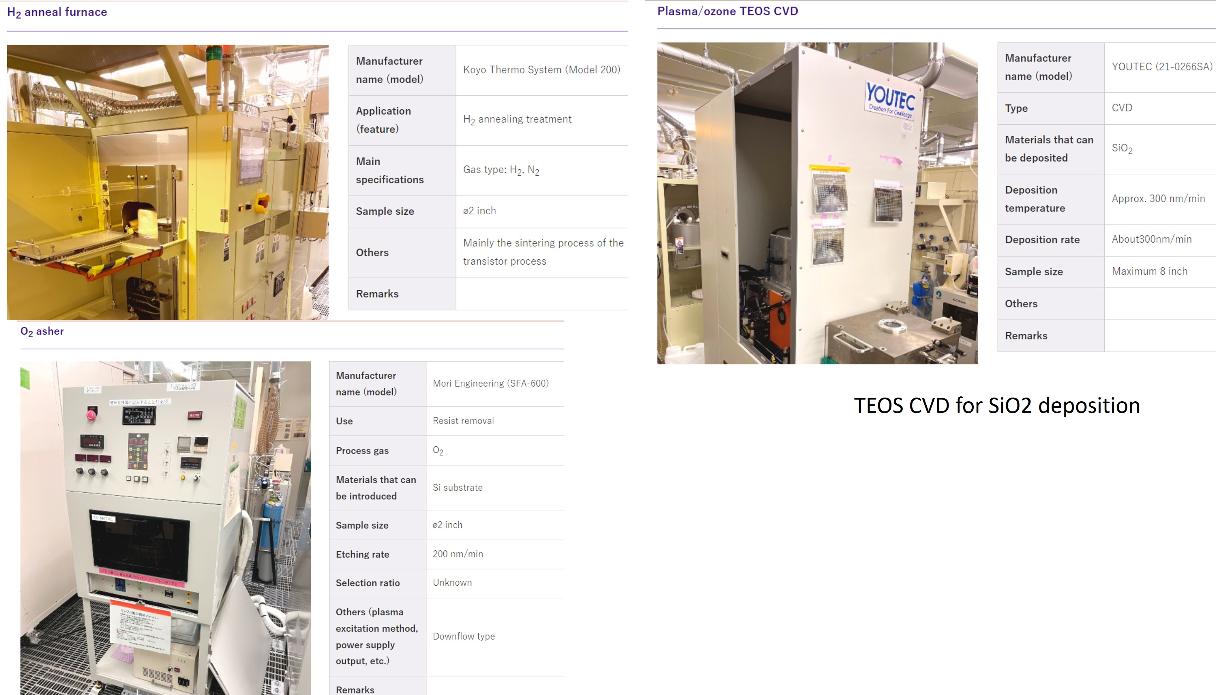
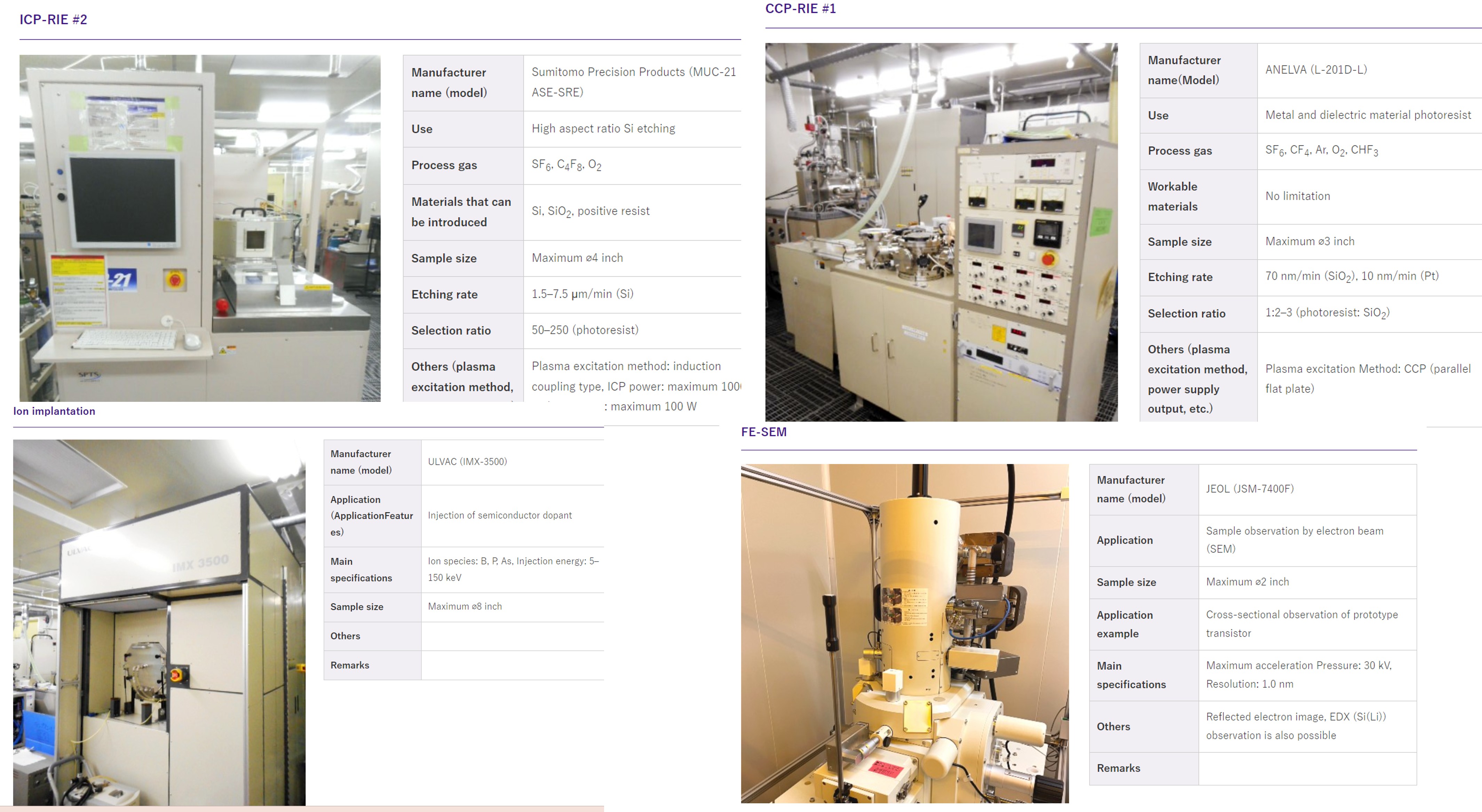
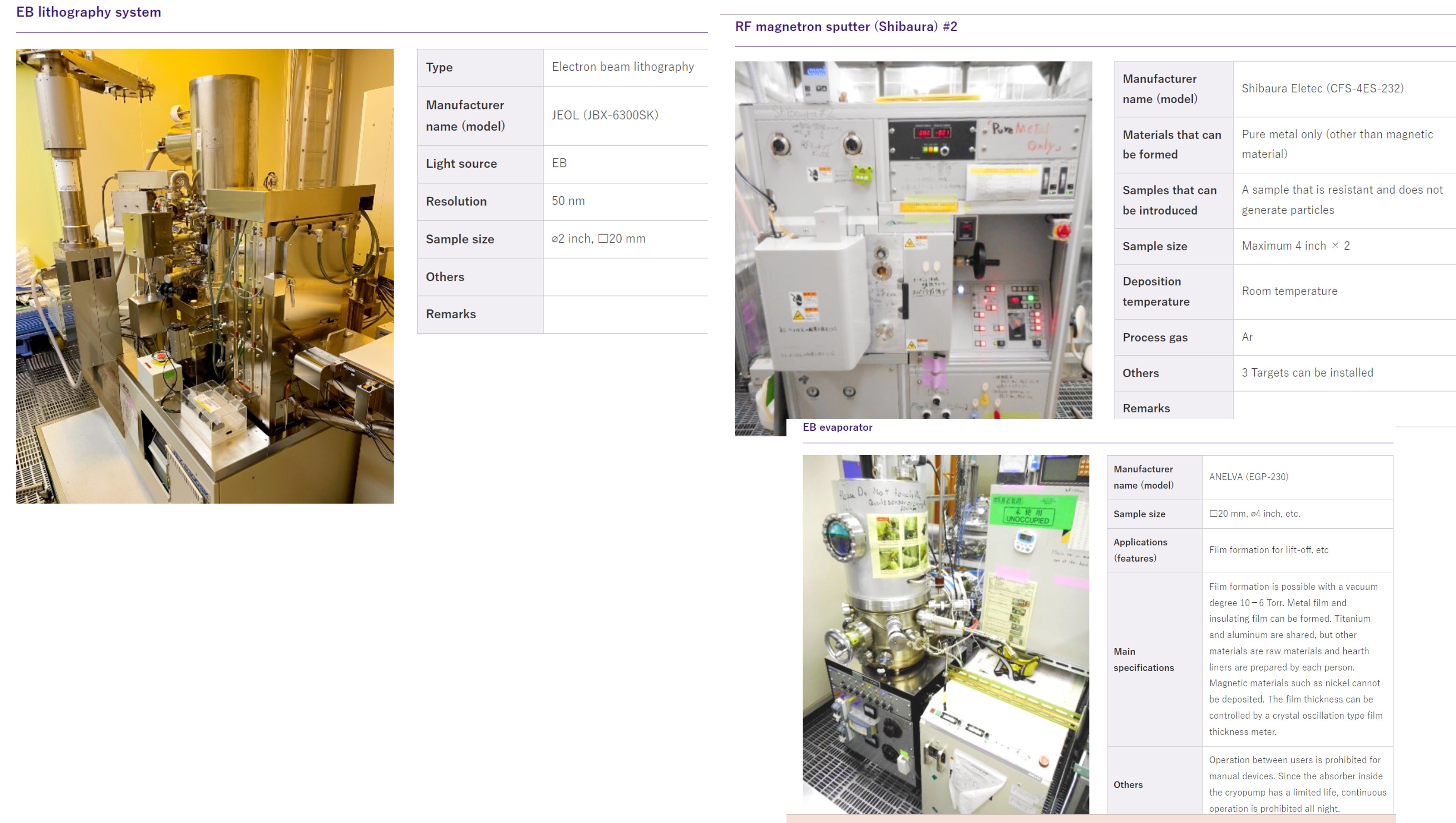
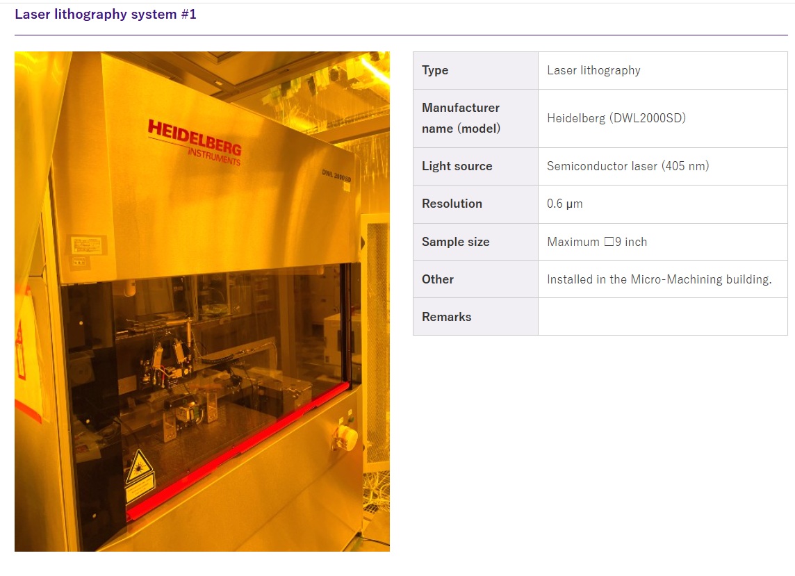
The transition from theoretical design to physical device required mastering an array of advanced cleanroom instrumentation. The fabrication workflow demanded sub-micron alignment precision and stringent contamination control. I utilized high-resolution photolithography tools, advanced deposition systems, and reactive ion etching platforms to pattern and transfer the intricate sensor geometries from the photomask onto the SOI wafer.
Ellipsometer (UVISEL)
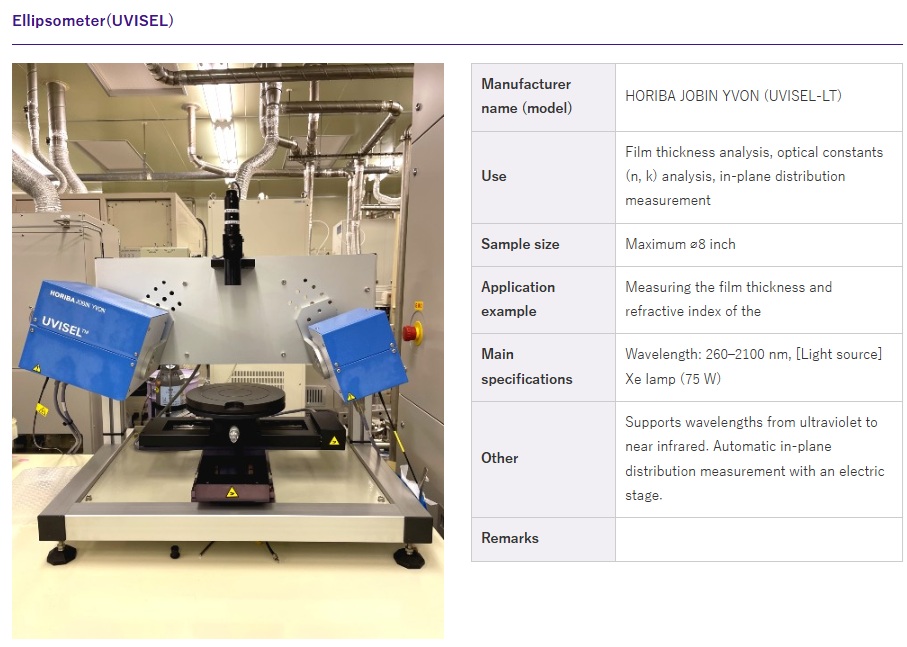
Ellipsometer (UVISEL)
Manufacturer name (model) HORIBA JOBIN YVON (UVISEL-LT)
Use Film thickness analysis, optical constants (n, k) analysis, in-plane distribution measurement
Sample size Maximum ø8 inch
Application example Measuring the film thickness and refractive index
Main specifications Wavelength: 260–2100 nm, [Light source] Xe lamp (75 W)
Other Supports wavelengths from ultraviolet to near infrared. Automatic in-plane distribution measurement with an electric stage.

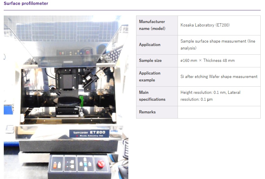
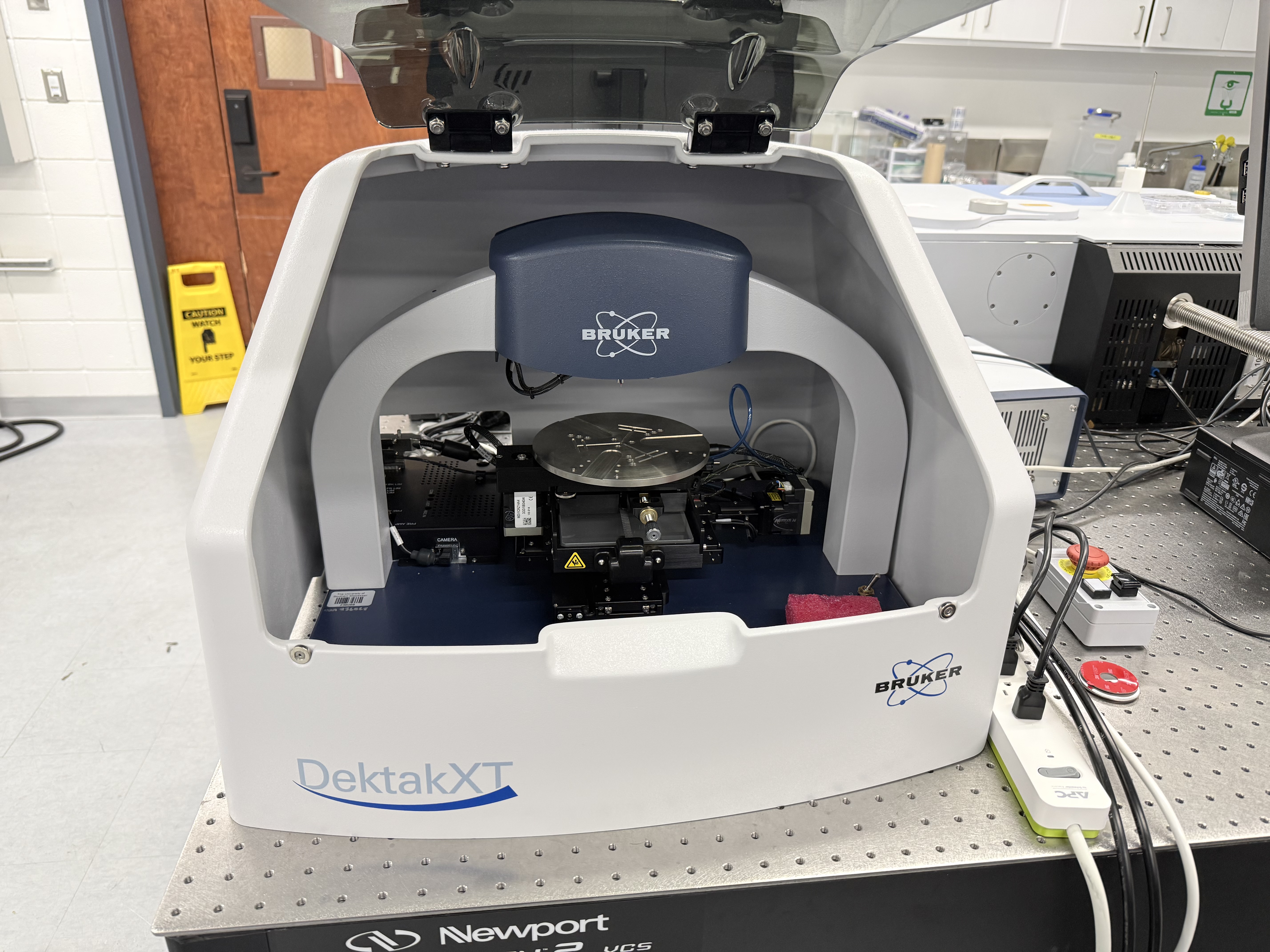
Surface Profilometer

Surface Profilometer
Manufacturer name (model) Kosaka Laboratory (ET200)
Application Sample surface shape measurement (line analysis)
Sample size ø160 mm × Thickness 48 mm
Application example Si after etching Wafer shape measurement
Main specifications Height resolution: 0.1 nm, Lateral resolution: 0.1 μm
Remarks

Ultraviolet Spectroscopic Ellipsometer (M-2000D-Tm)
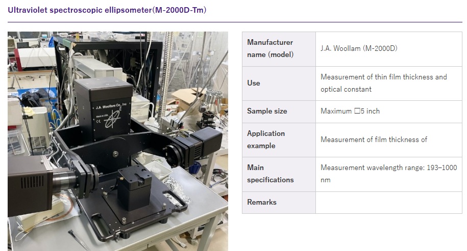
Ultraviolet Spectroscopic Ellipsometer
Manufacturer name (model) J.A. Woollam (M-2000D)
Use Measurement of thin film thickness and optical constant
Sample size Maximum ◻5 inch
Application example Measurement of film thickness of
Main specifications Measurement wavelength range: 193–1000 nm
Remarks

Fabrication & Process Optimization

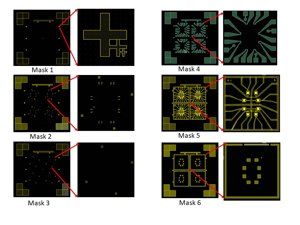
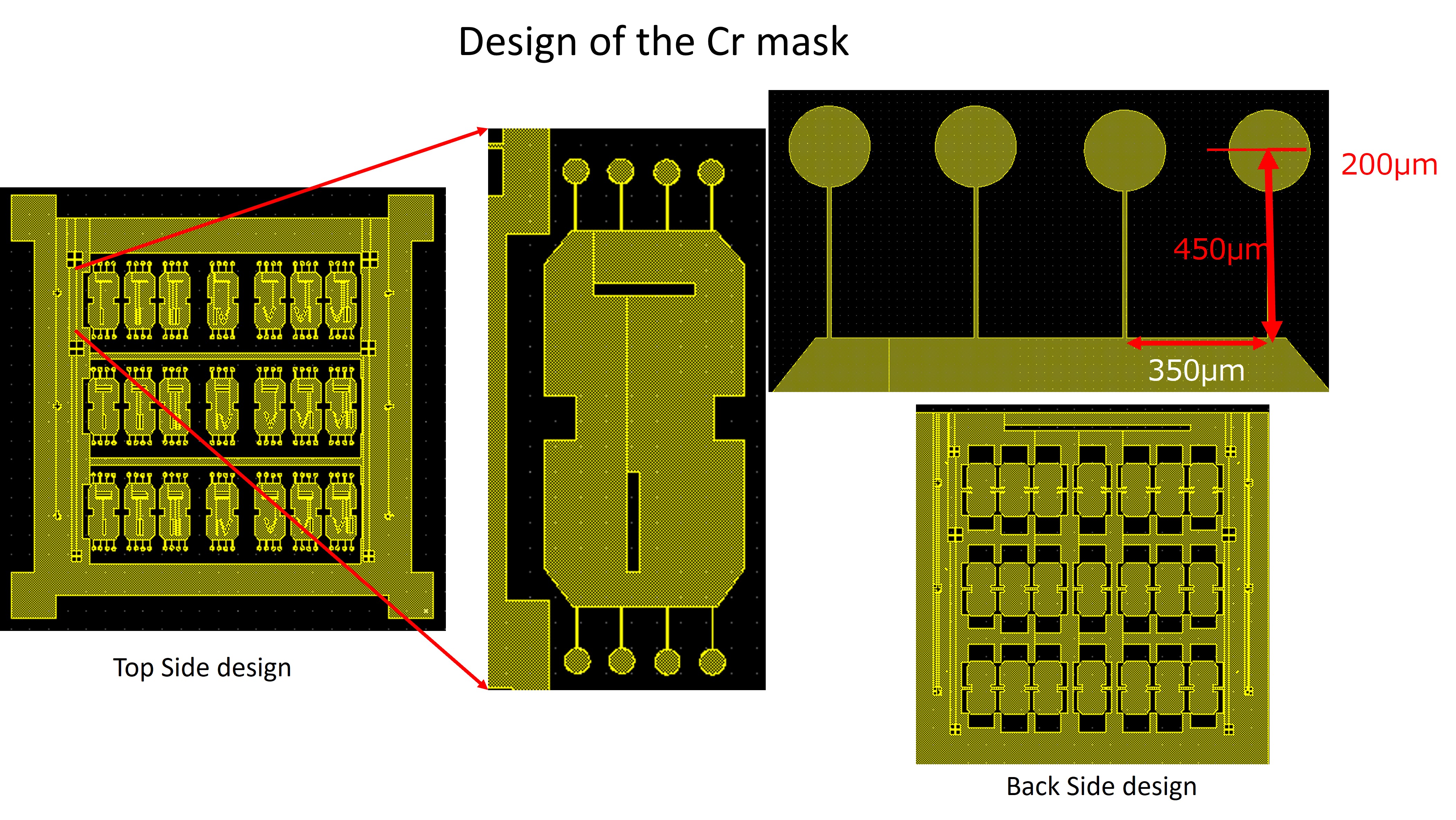
Cr Mask Design Using Layout Software

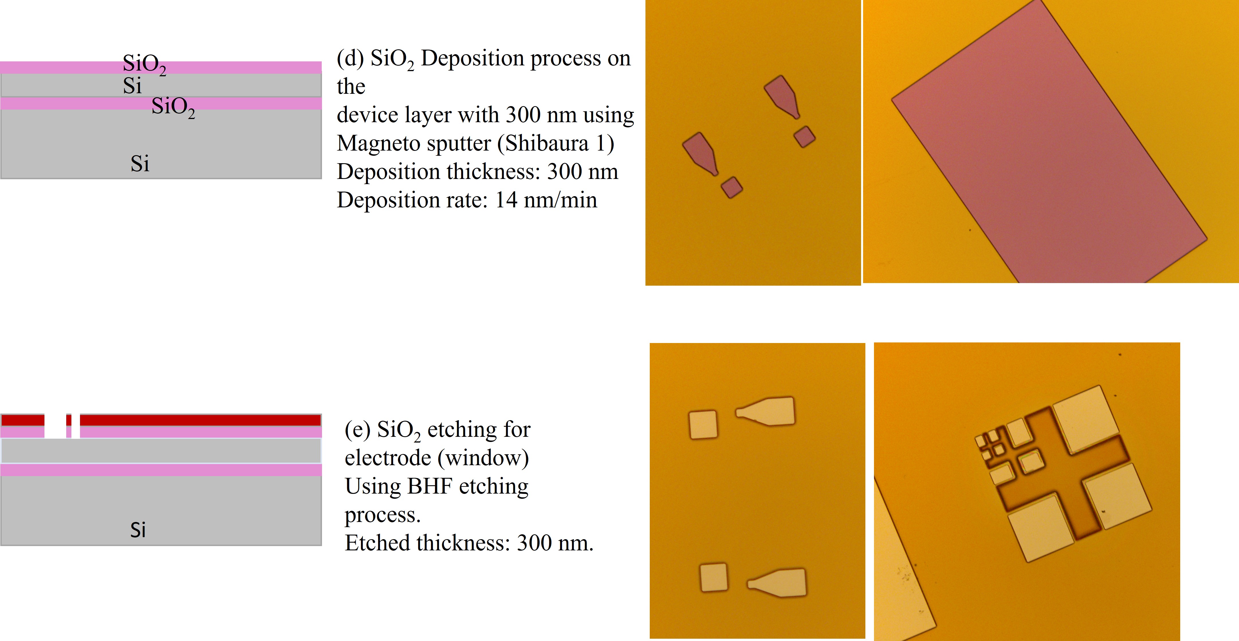
Designed the complete six-layer chromium (Cr) mask set using layout design software for MEMS fabrication of the nanomechanical gas sensor. The mask layers included alignment marks, ion implantation regions, silicon etching patterns, metallization, backside etching windows, and structural release features.

The layout was developed to support accurate multi-layer alignment on SOI wafers and reliable transfer of micron-scale sensor geometries during lithography.
Process Execution & DRIE Optimization

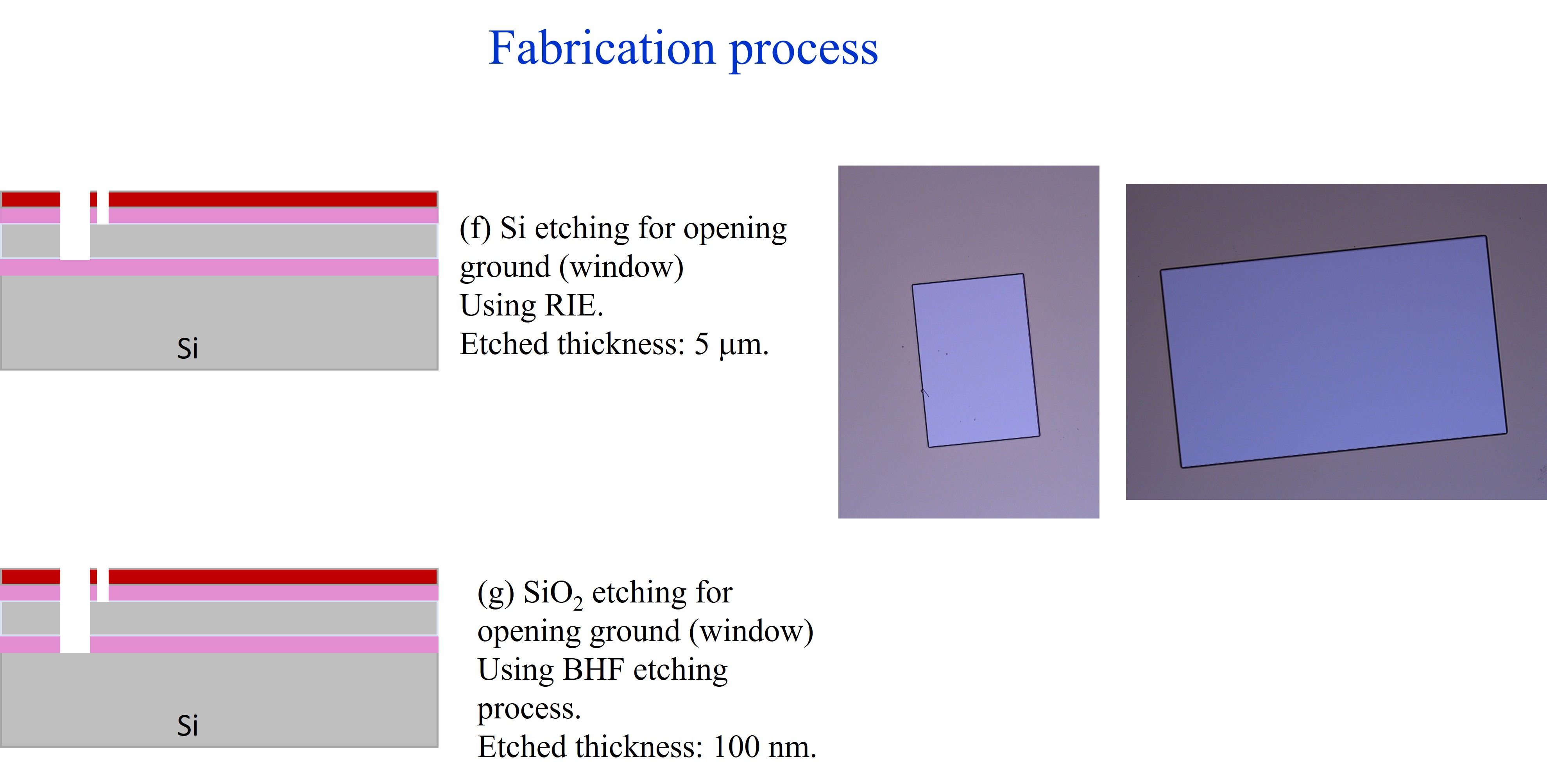
Translating the sensor design into silicon was an iterative and highly rigorous process. Optimization of the Deep Reactive-Ion Etching (DRIE) parameters was paramount to achieving vertical sidewall profiles for the suspended Si slits without inducing micro-trenching or undercutting. I systematically documented each process variable—gas flow rates, RF power, and chamber pressure—conducting failure analysis at each step to refine the process recipe. This structured Design of Experiments (DOE) approach ultimately led to a repeatable, high-yield fabrication sequence suitable for commercial scaling.
Troubleshooting & Process Optimization: Improving Polymer Deposition Uniformity for Enhanced Sensor Performance

Challenge: Poor Sensitivity and Inconsistent Sensor Response

During early device evaluation, the nanomechanical gas sensors exhibited inconsistent sensitivity and poor repeatability between fabricated devices. Although the MEMS structures were successfully fabricated, the sensor responses varied significantly from chip to chip, preventing reliable gas discrimination and limiting commercial scalability.

Root Cause Investigation

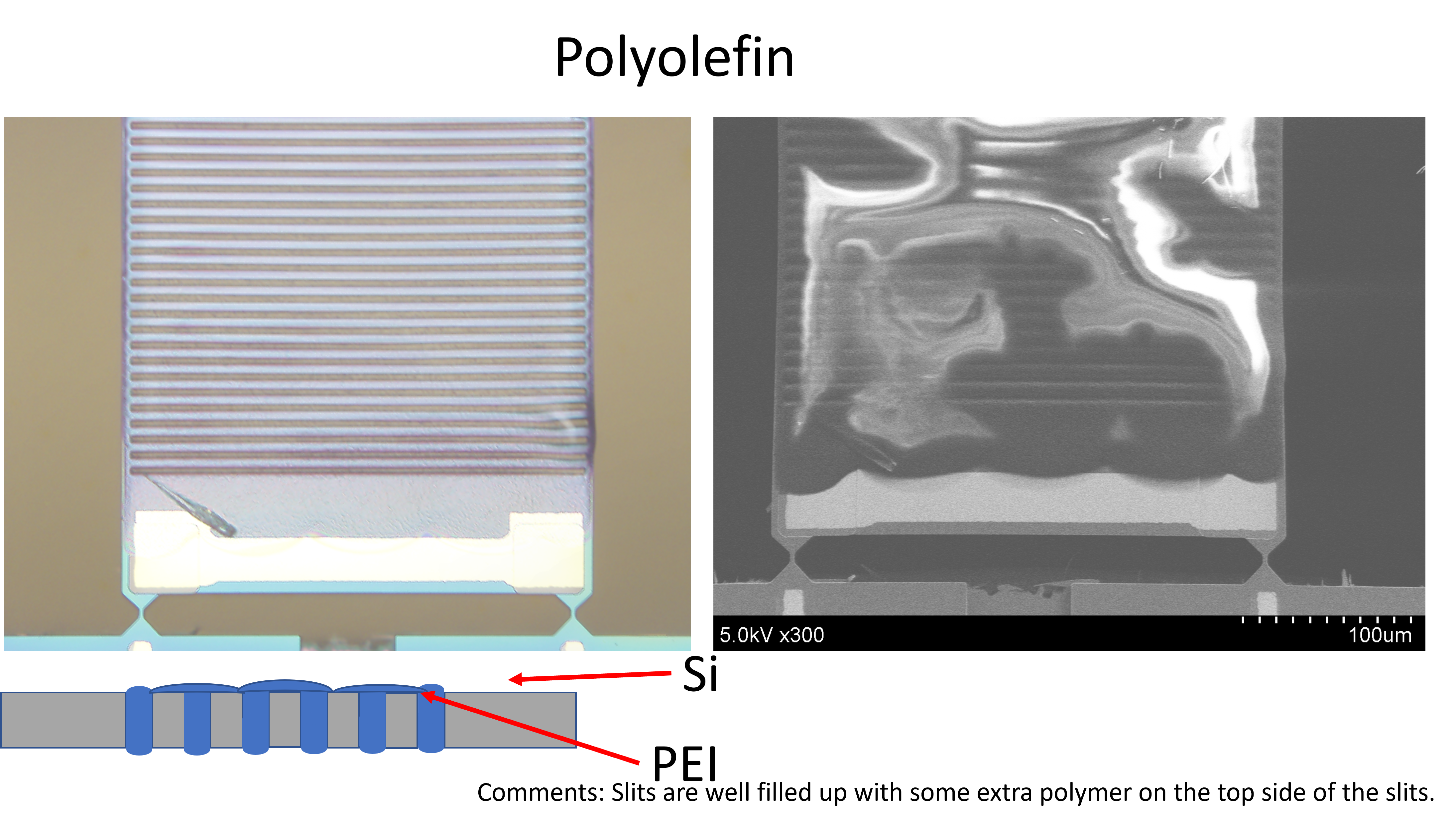
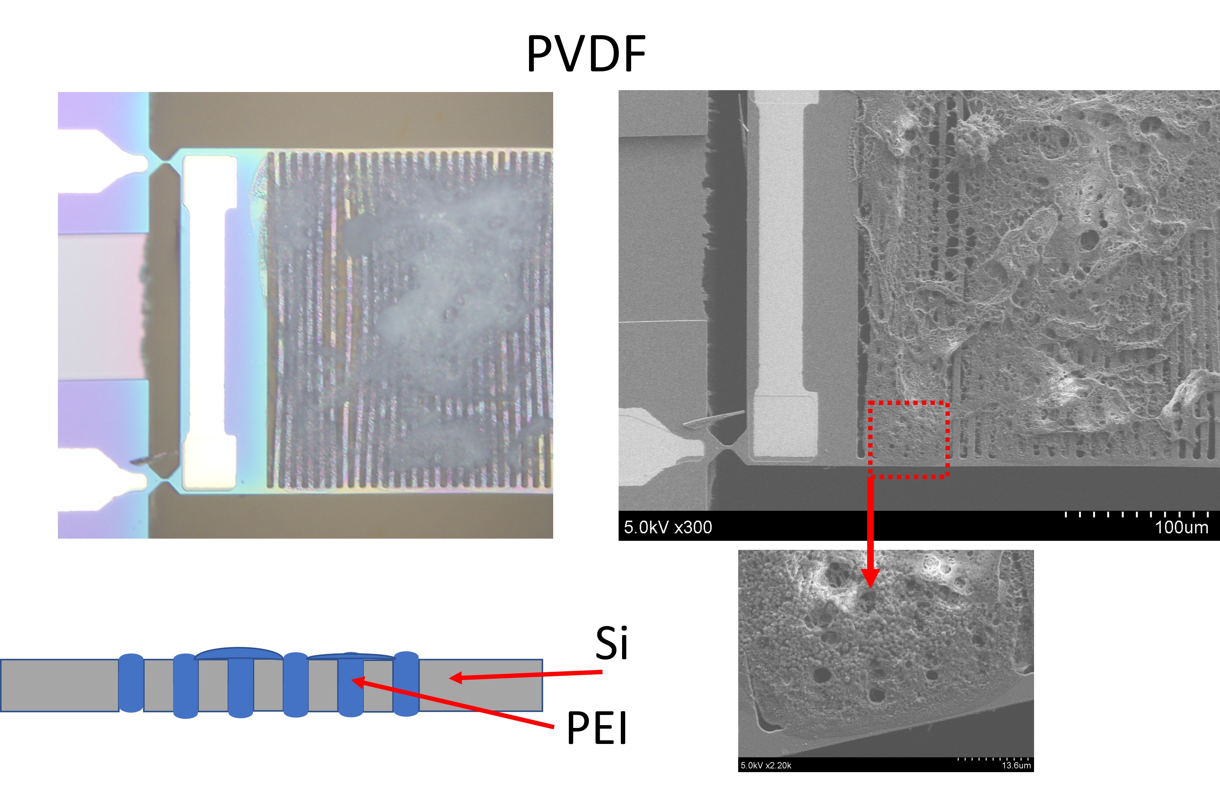
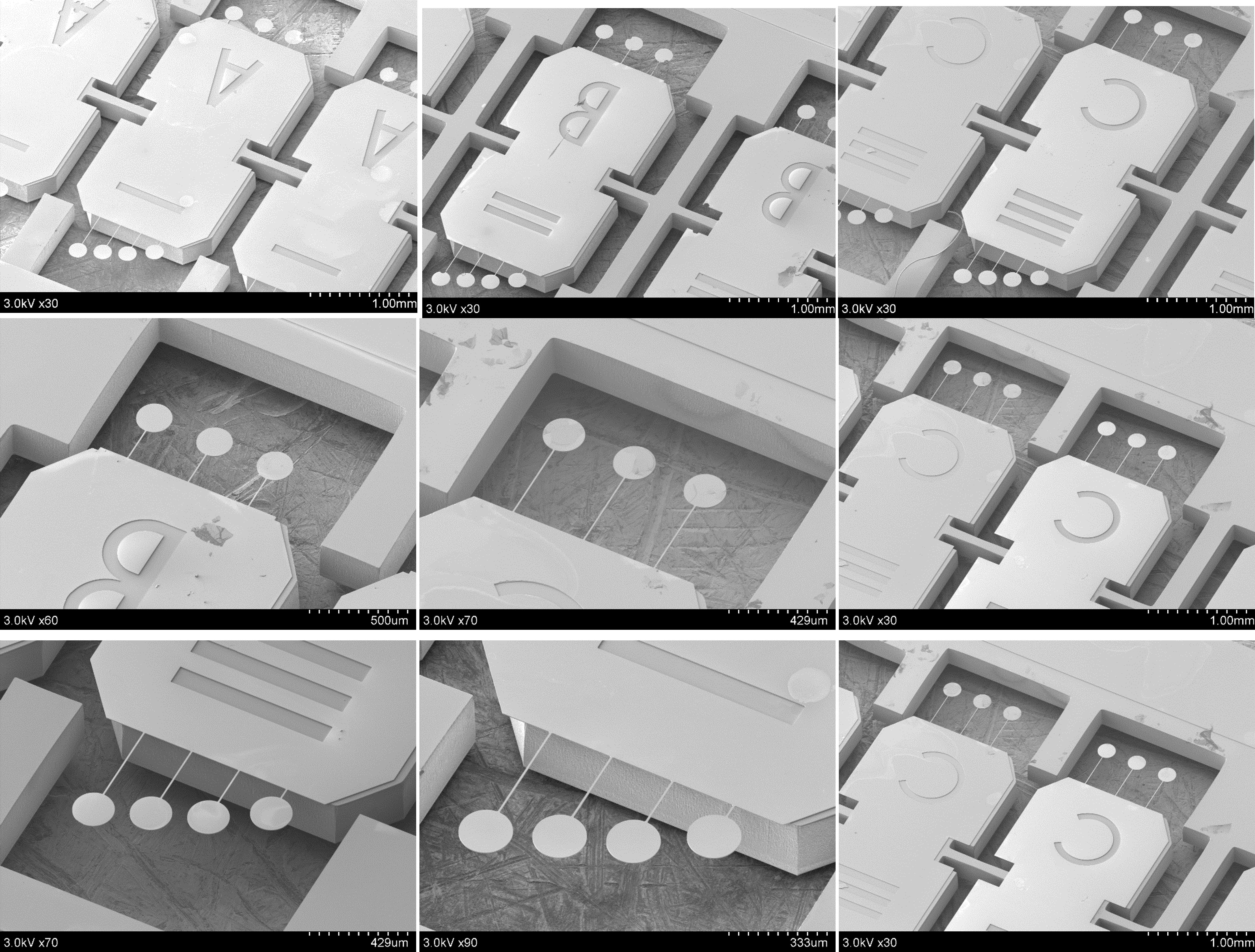
To identify the source of variability, I conducted a metrology-driven failure analysis using optical microscopy and scanning electron microscopy (SEM).

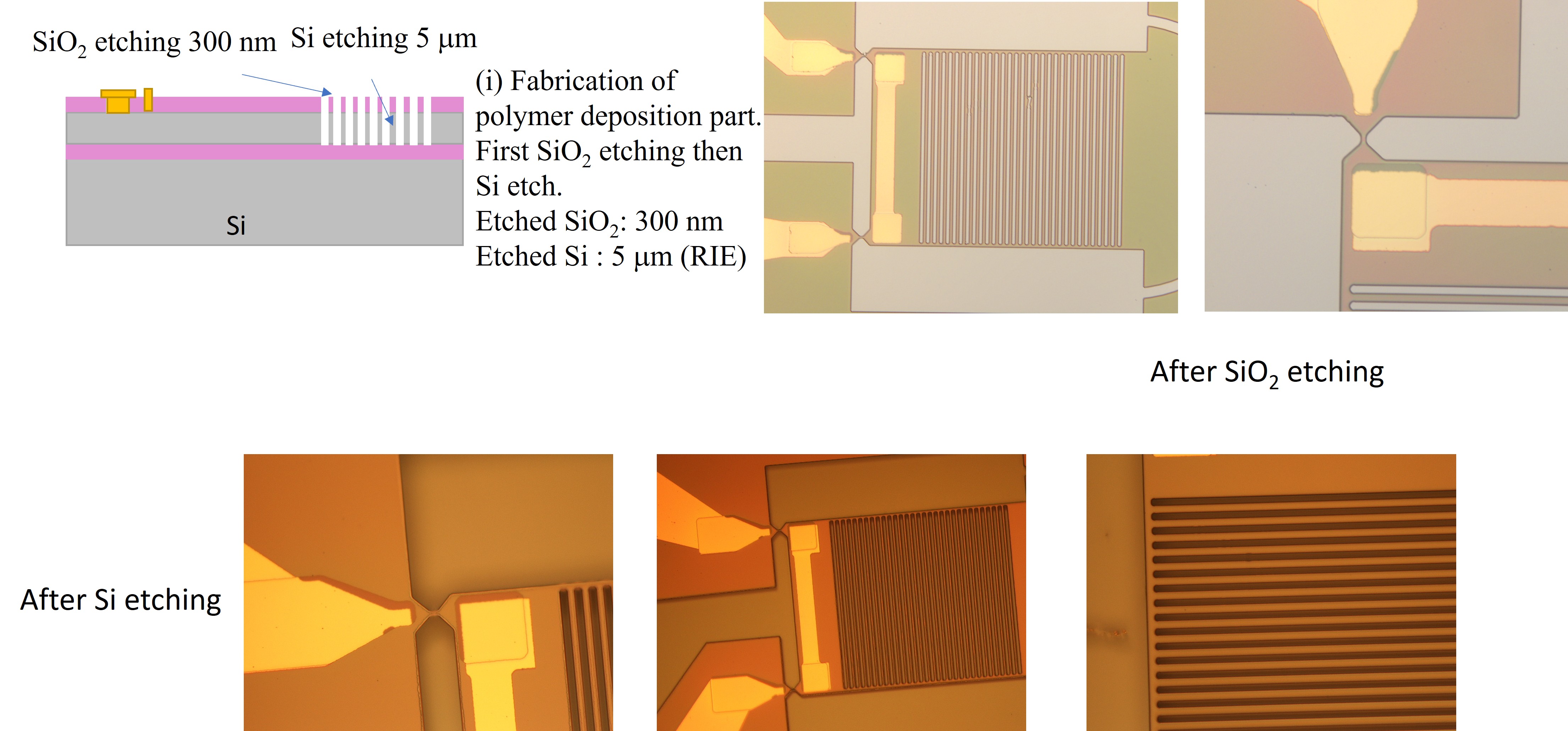
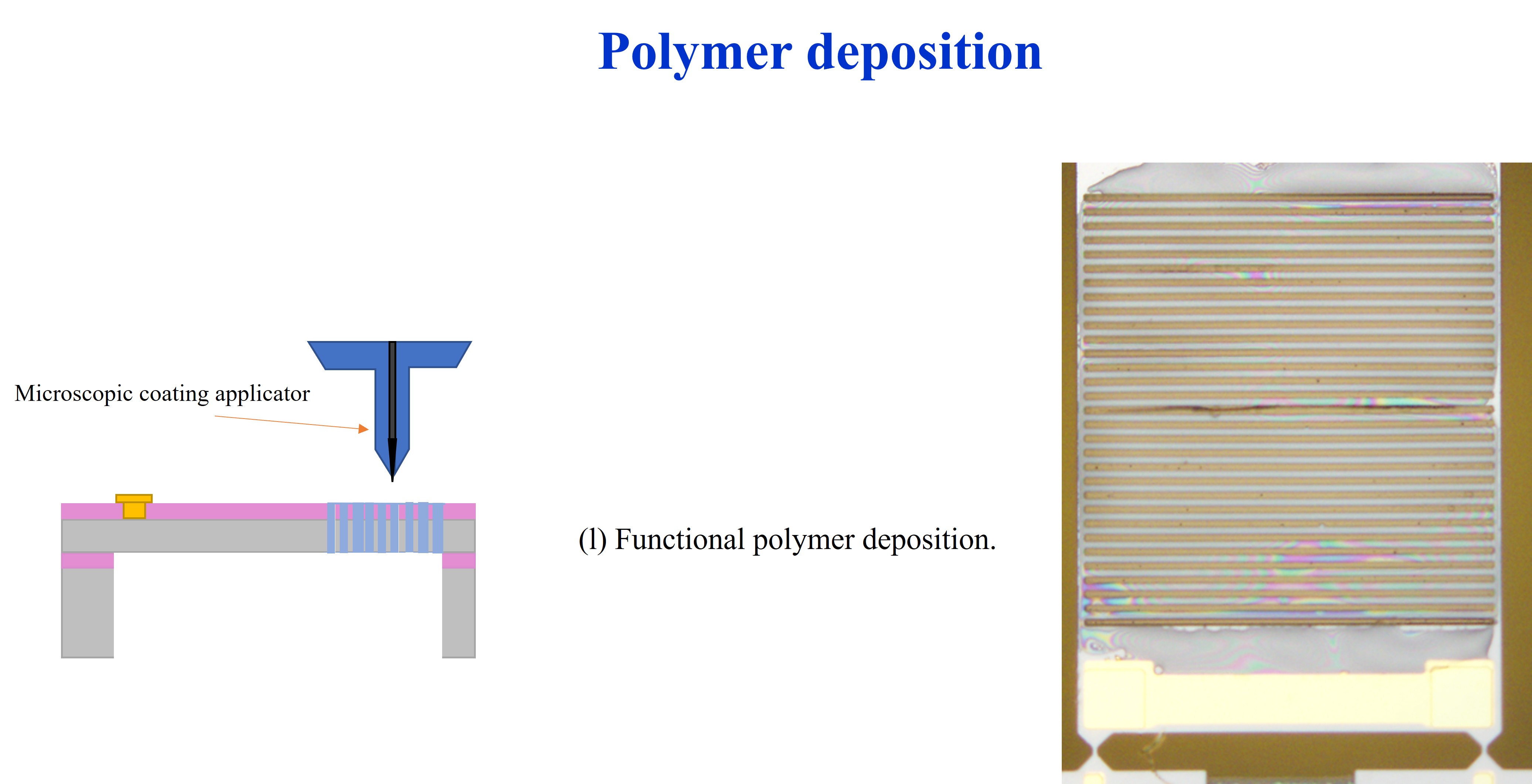
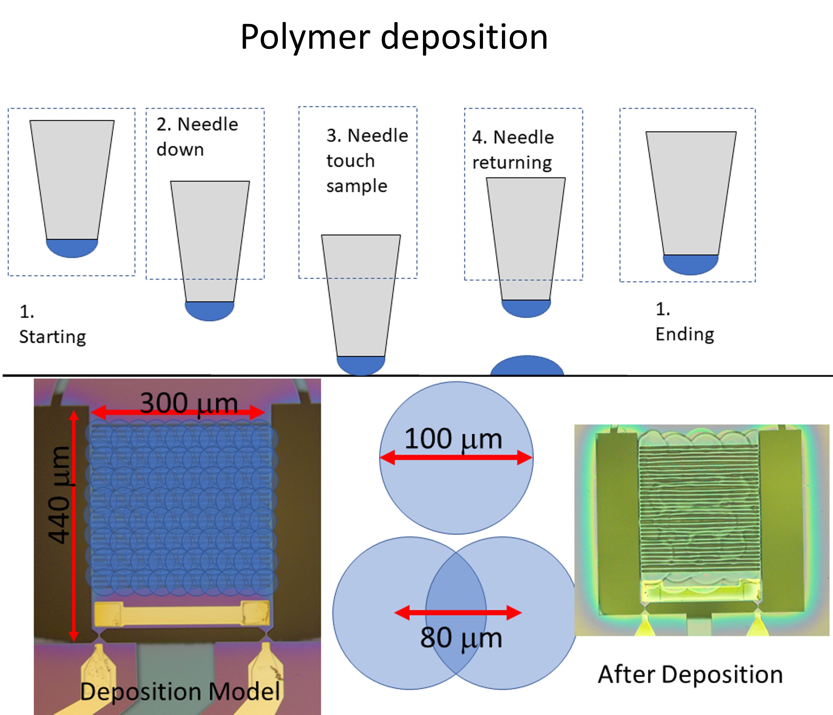
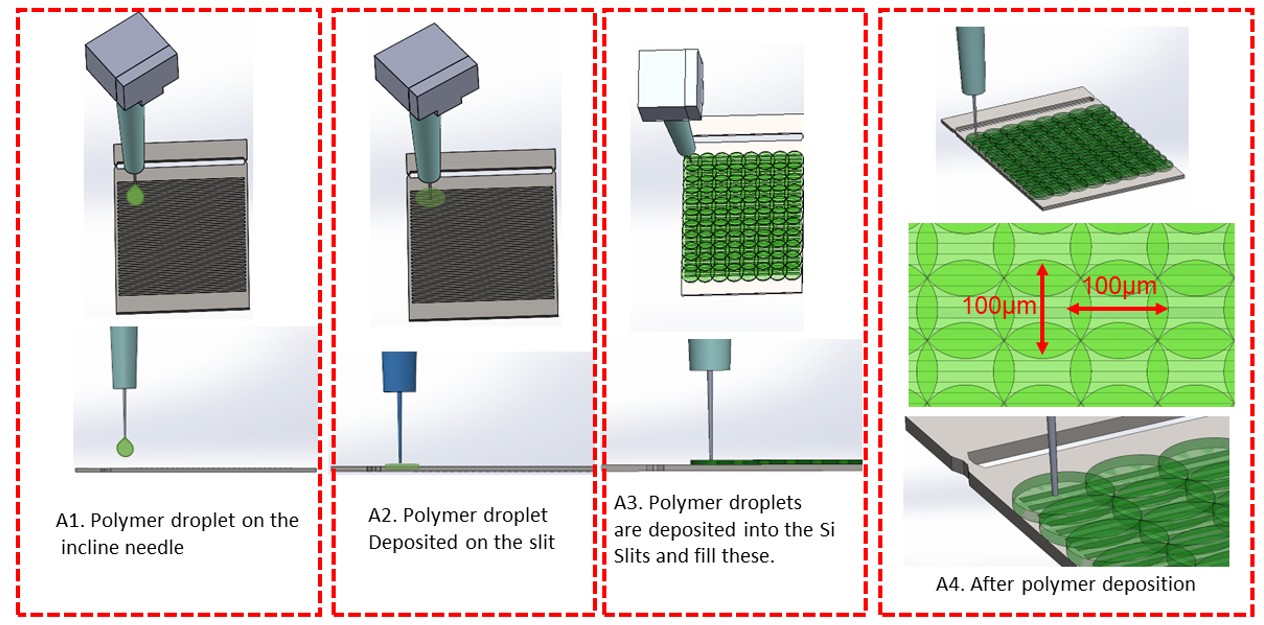
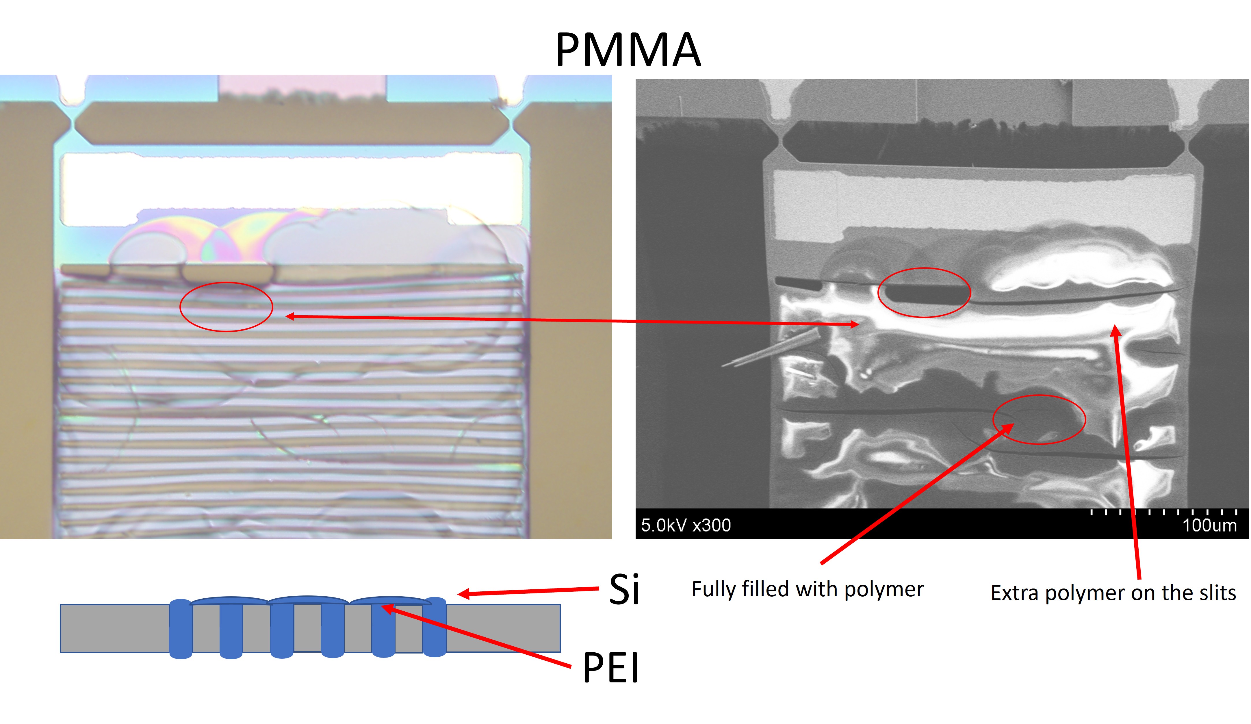
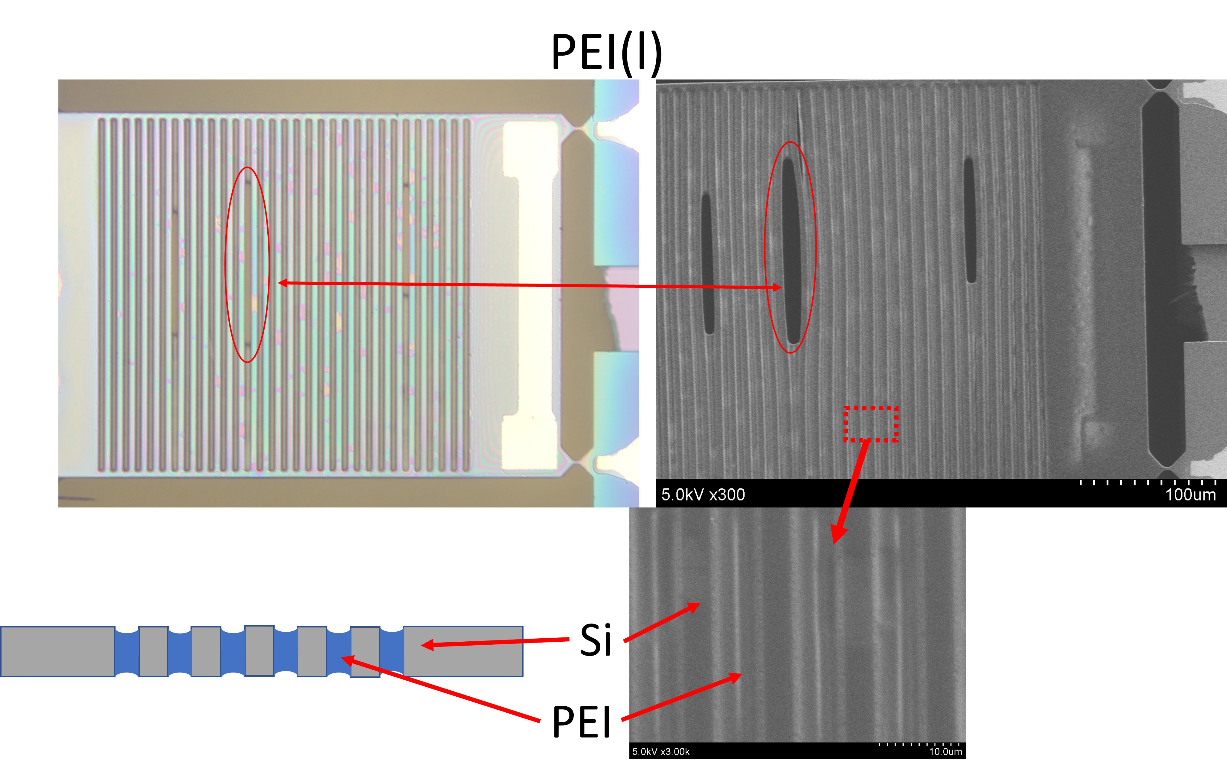
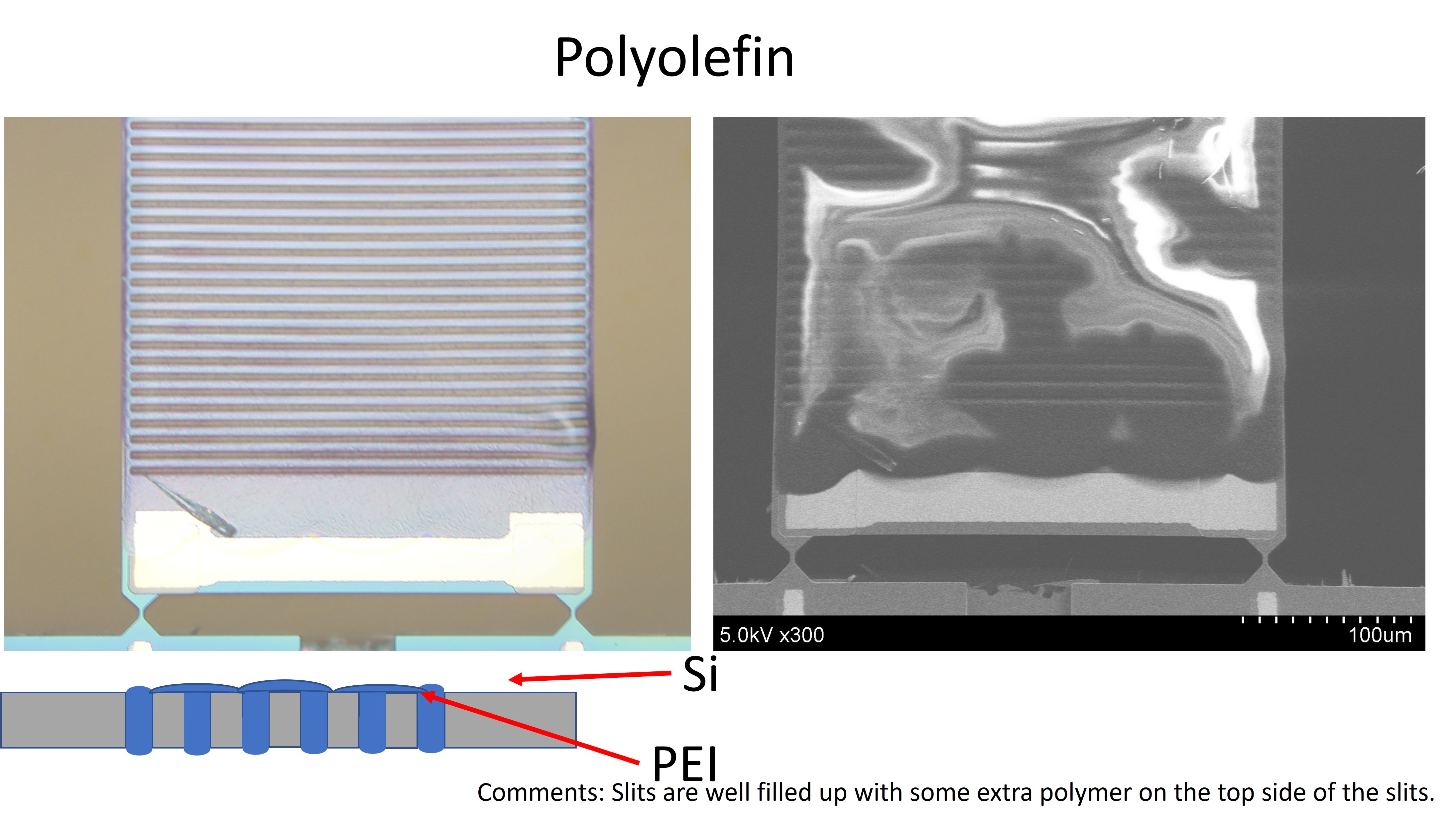
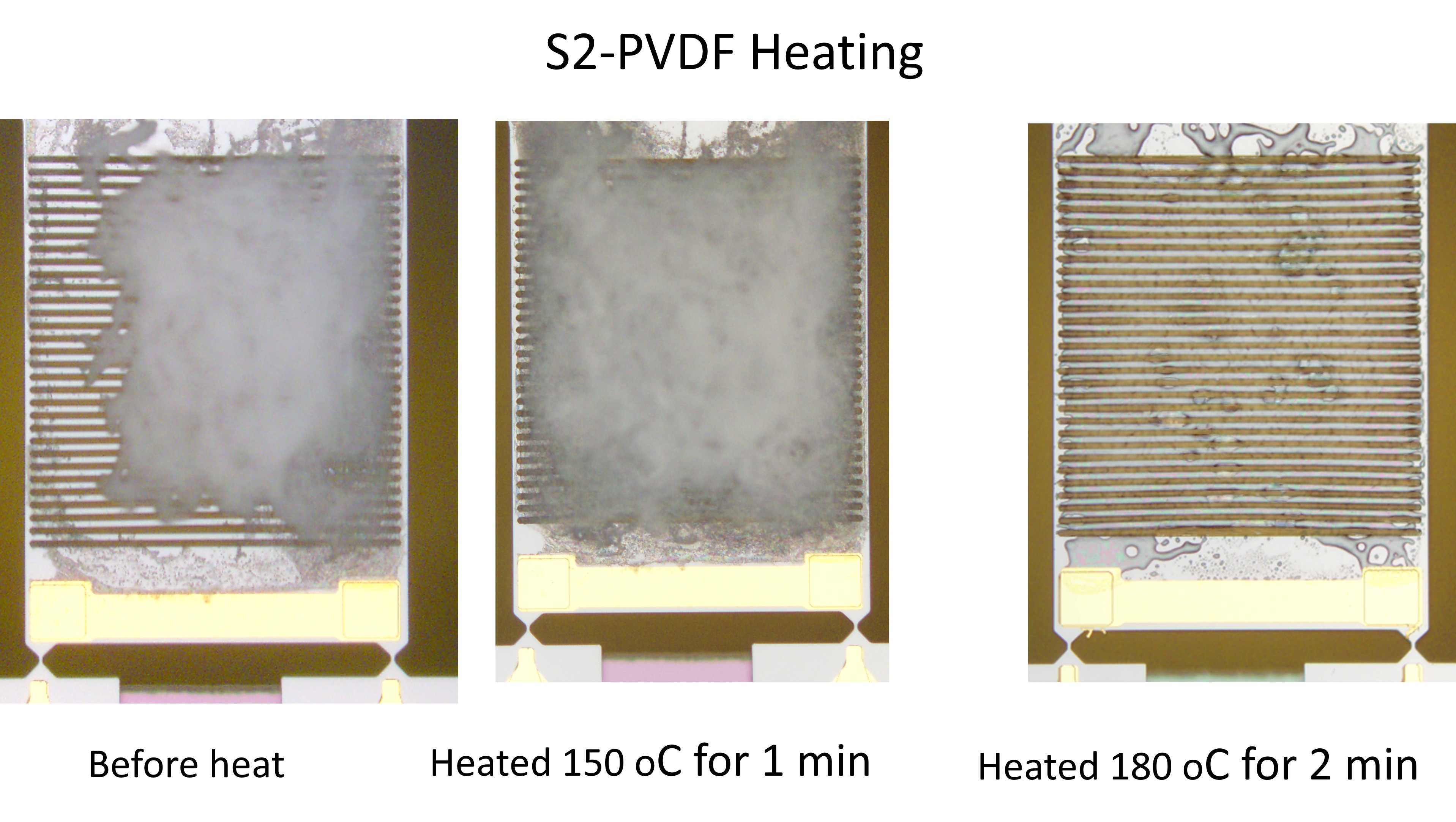
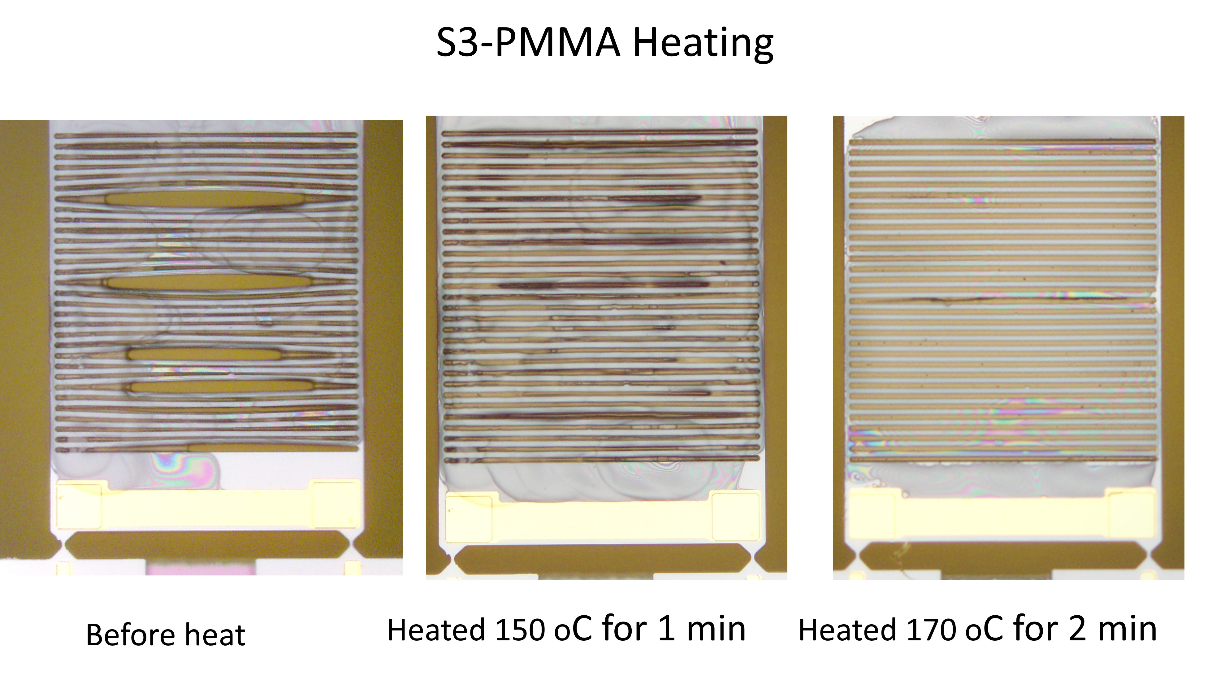
The investigation revealed that the primary issue originated from the polymer deposition process. Different sensing polymers exhibited significantly different wetting and filling behaviors inside the suspended silicon slit structures:

  • Some polymers partially filled the slits, leaving uncovered regions and reducing active sensing volume.
  • Other polymers excessively accumulated on top of the slit structures, creating thick surface layers that reduced mechanical sensitivity.
  • Non-uniform filling caused variations in stress transfer between gas-induced polymer swelling and the piezoresistive silicon structures.
  • Device-to-device reproducibility was severely affected because identical deposition parameters produced different polymer morphologies.

Cross-sectional SEM analysis confirmed that polymer distribution inside the micron-scale silicon slits was highly dependent on polymer viscosity, surface tension, and curing conditions.

Engineering Solution

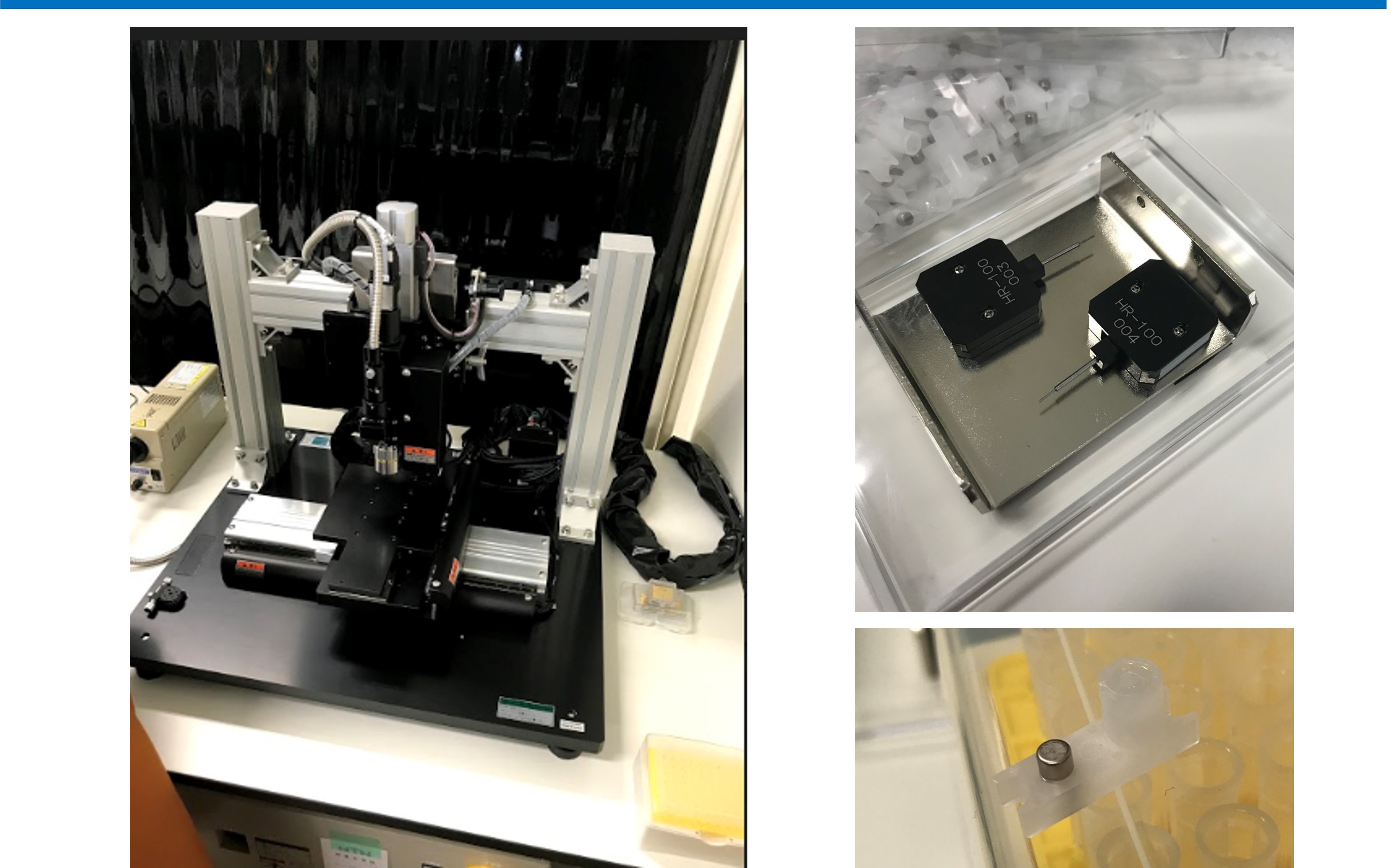
To overcome this challenge, I systematically optimized the post-deposition thermal treatment process for each polymer individually.

Rather than using a single curing protocol for all materials, I developed polymer-specific heating profiles based on the thermal properties and melting behavior of each sensing material. The optimization strategy involved:

  • Characterizing polymer morphology using optical microscopy and SEM.
  • Identifying void formation, incomplete filling, and excessive surface accumulation.
  • Heating each polymer above its characteristic softening or melting temperature.
  • Allowing controlled polymer reflow to improve penetration into the silicon slits.
  • Optimizing heating temperature and duration to maximize uniformity while preserving device integrity.

Results

The optimized thermal reflow process significantly improved polymer distribution throughout the sensing structures. After optimization:

  • Silicon slits were filled more uniformly.
  • Uncovered sensing regions were eliminated.
  • Excess polymer accumulation was minimized.
  • Device-to-device variability was reduced.
  • Sensor repeatability and reproducibility improved substantially.
  • Mechanical coupling between polymer swelling and silicon transducers became more consistent.
  • Gas sensitivity increased due to improved active sensing volume and more efficient stress transfer.

This troubleshooting effort transformed polymer deposition from a major source of process variation into a repeatable and manufacturable fabrication step, contributing significantly to the successful commercialization pathway of the nanomechanical gas sensor platform.
Finite Element Analysis (FEA) by COMSOL: Stress Transfer

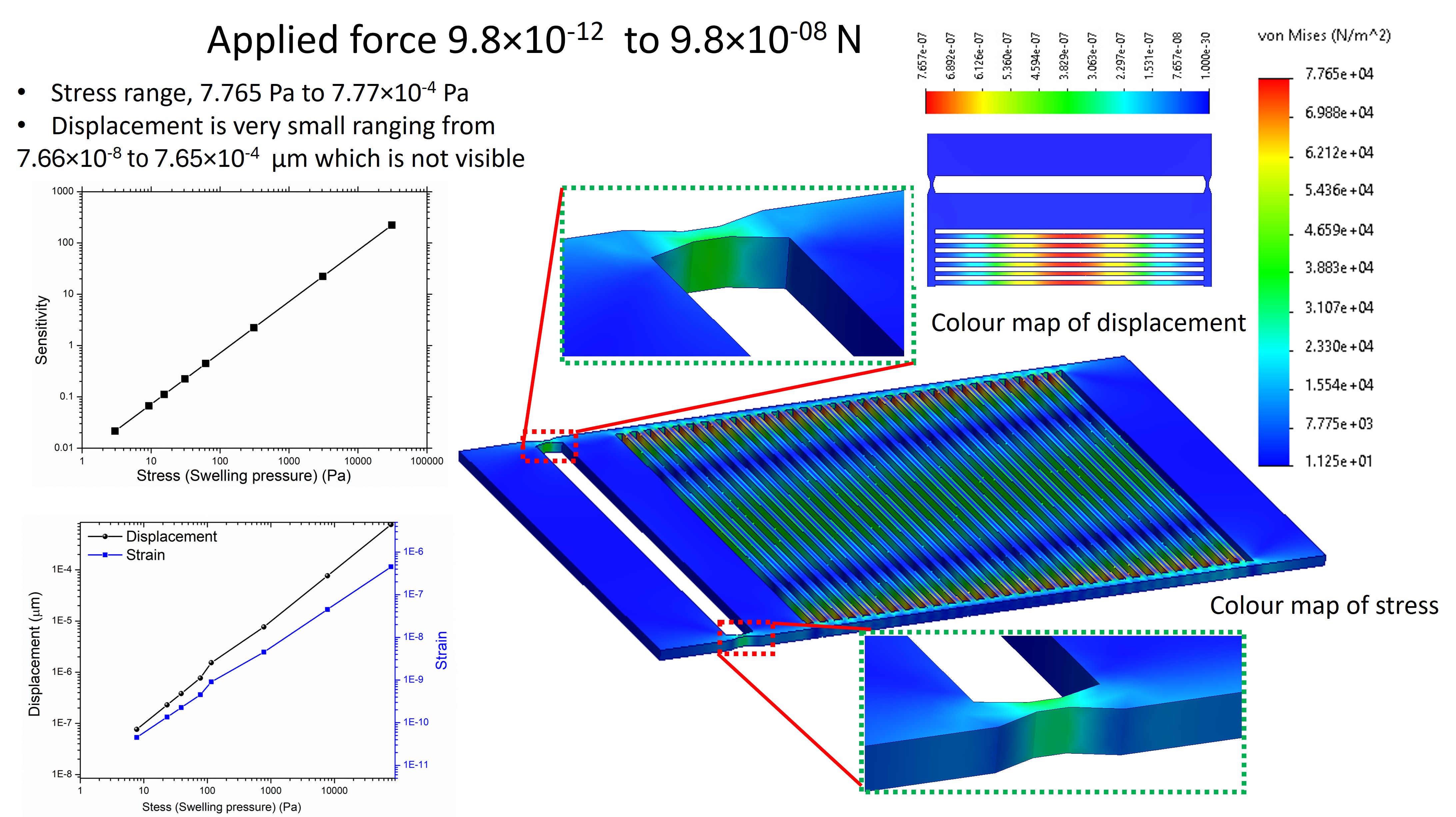
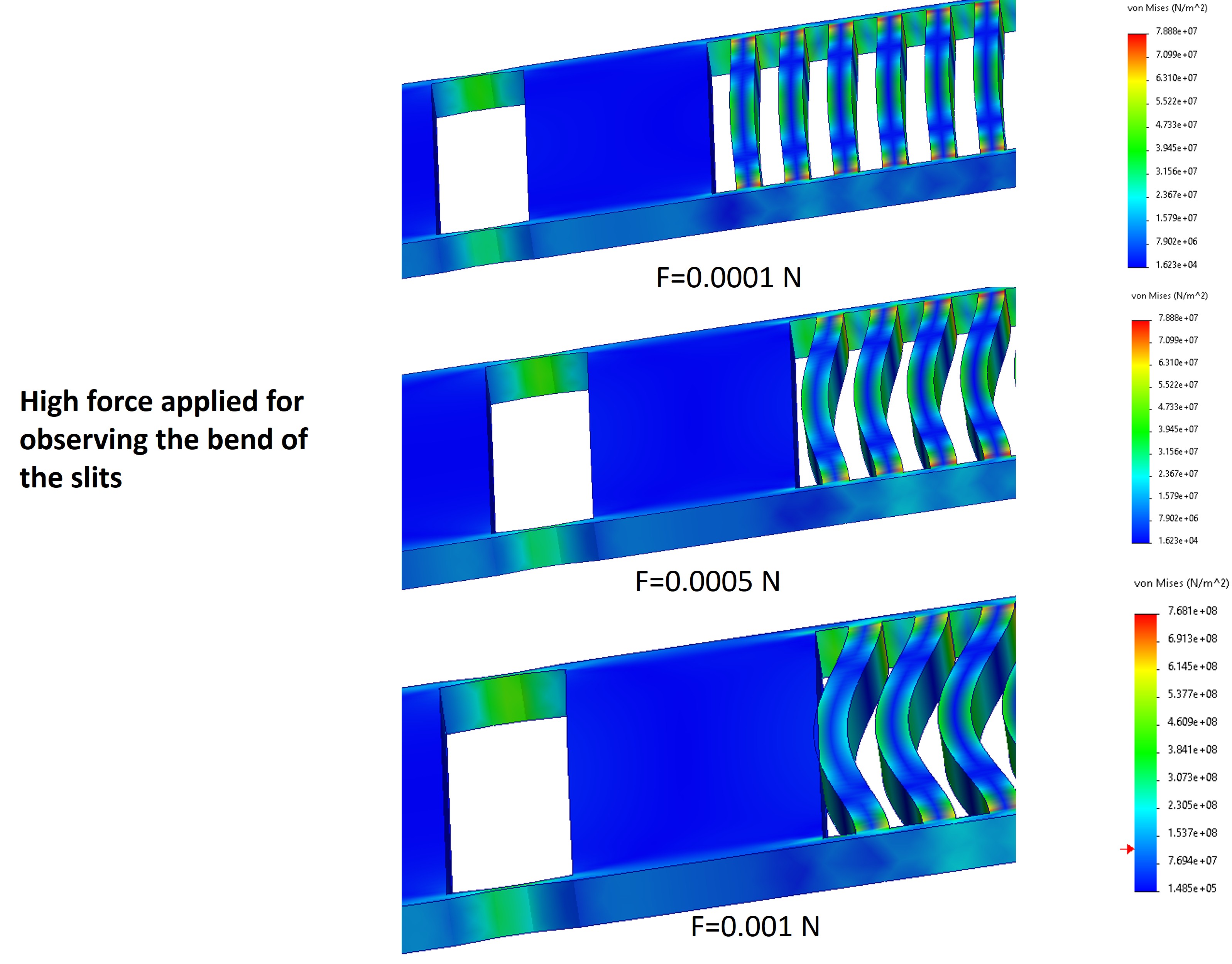
Prior to physical fabrication and to understand the micromechanical behavior of the sensor, I conducted Finite Element Analysis (FEA) using COMSOL Multiphysics. This simulation modeled the stress distribution across the suspended silicon structure during polymer swelling. By visualizing the stress concentration points and the efficiency of stress transfer from the functional polymer to the piezoresistive elements, I was able to validate the geometrical design and predict the theoretical sensitivity of the nanomechanical array.
Device Assembly, Electronics & Metrology

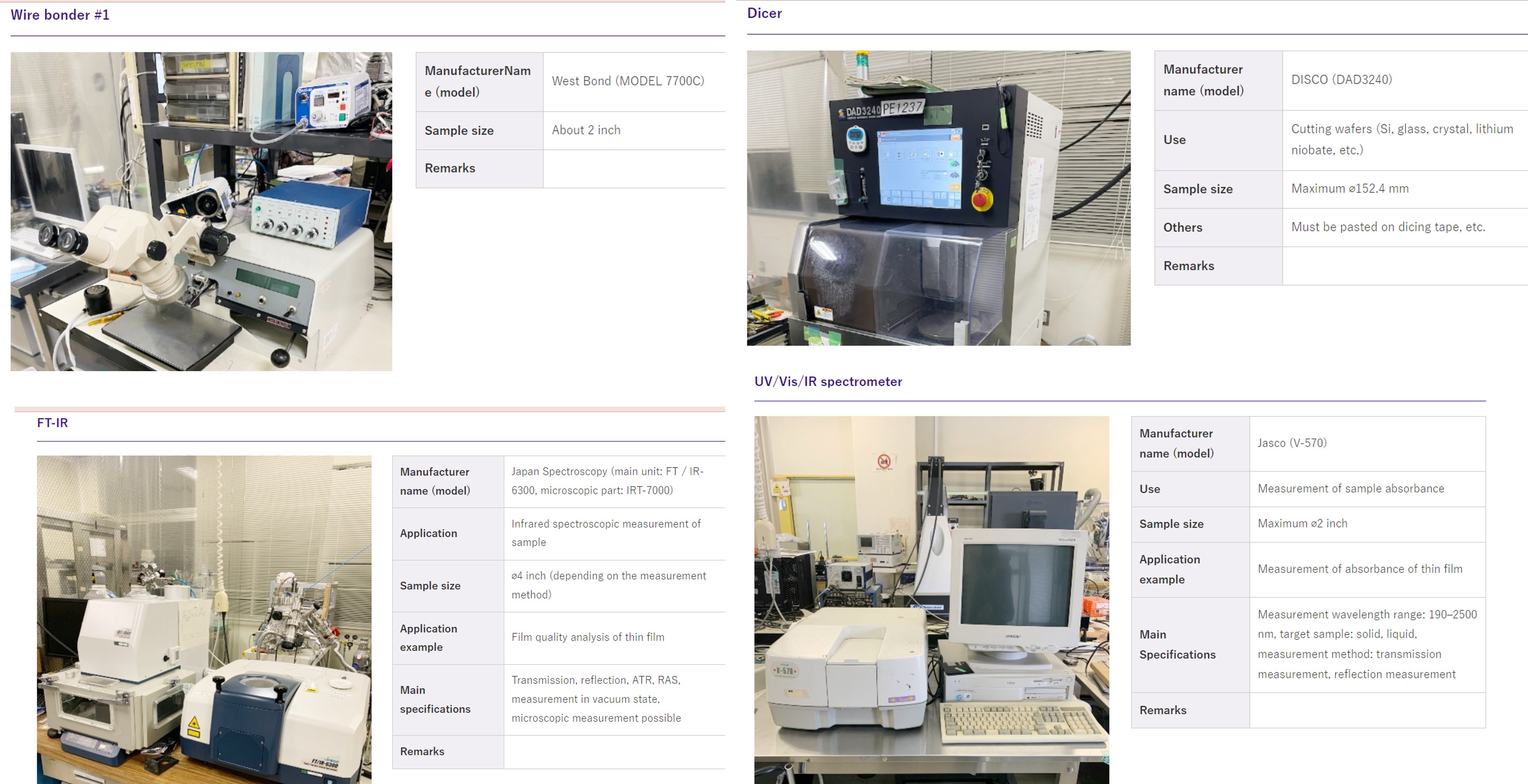
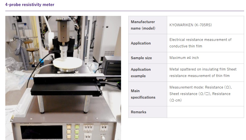
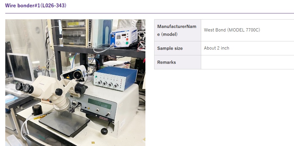
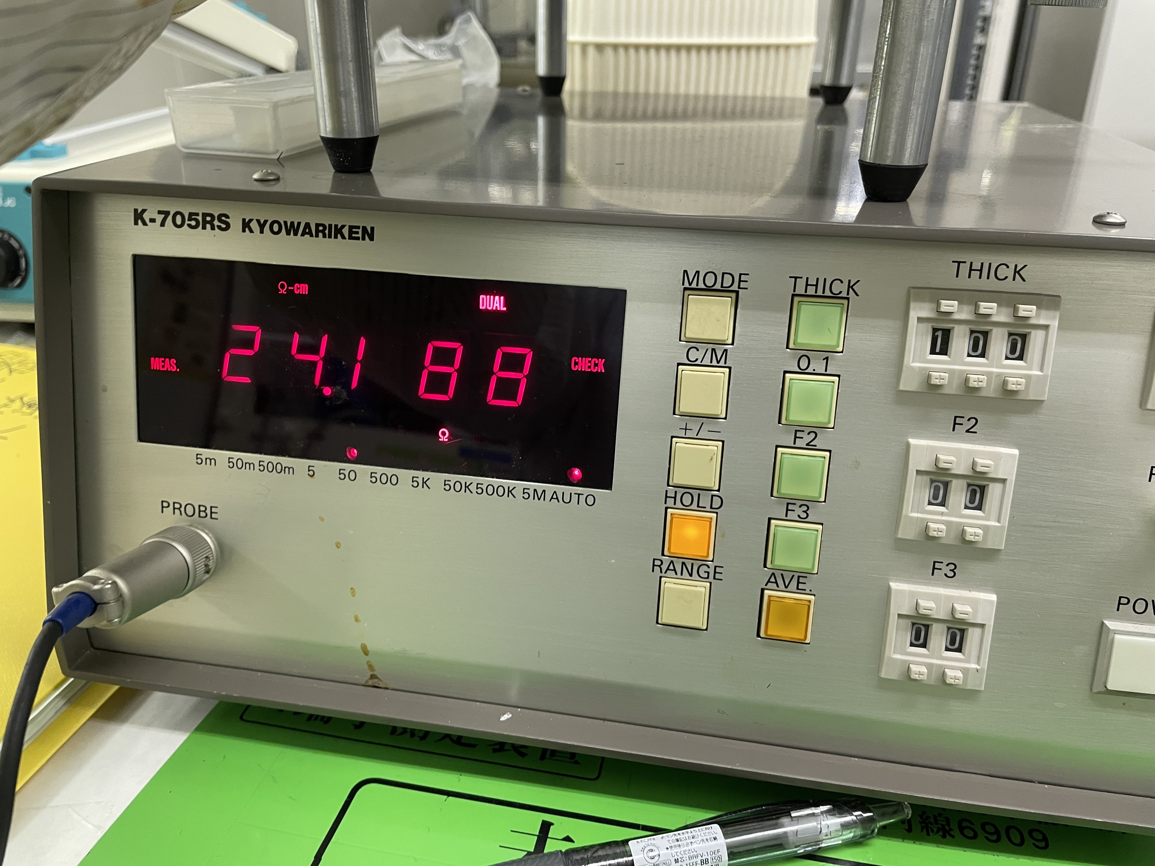
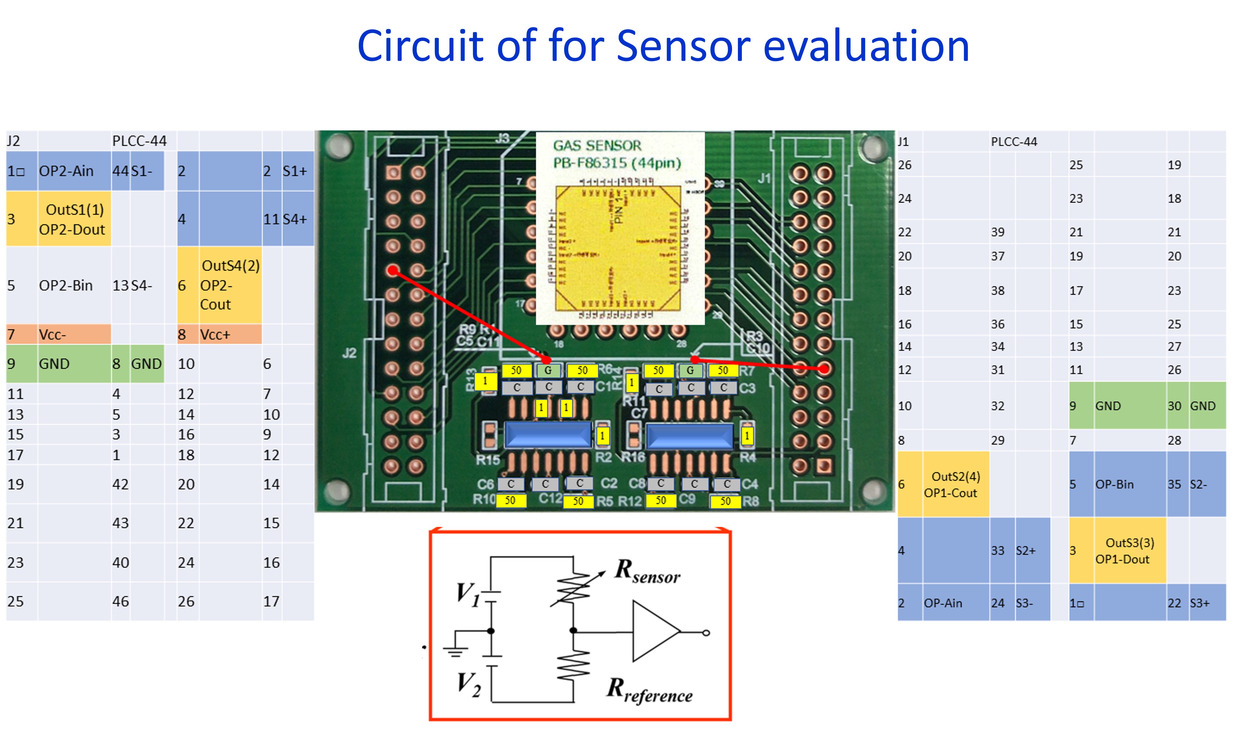
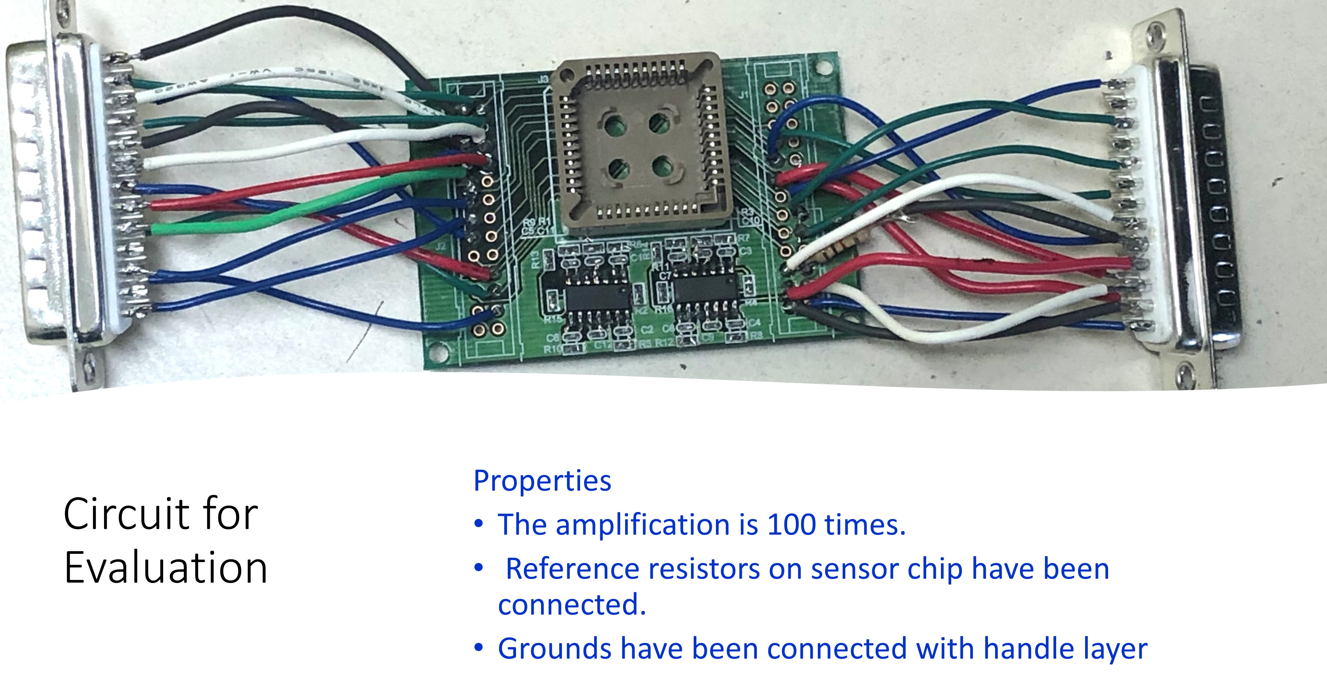
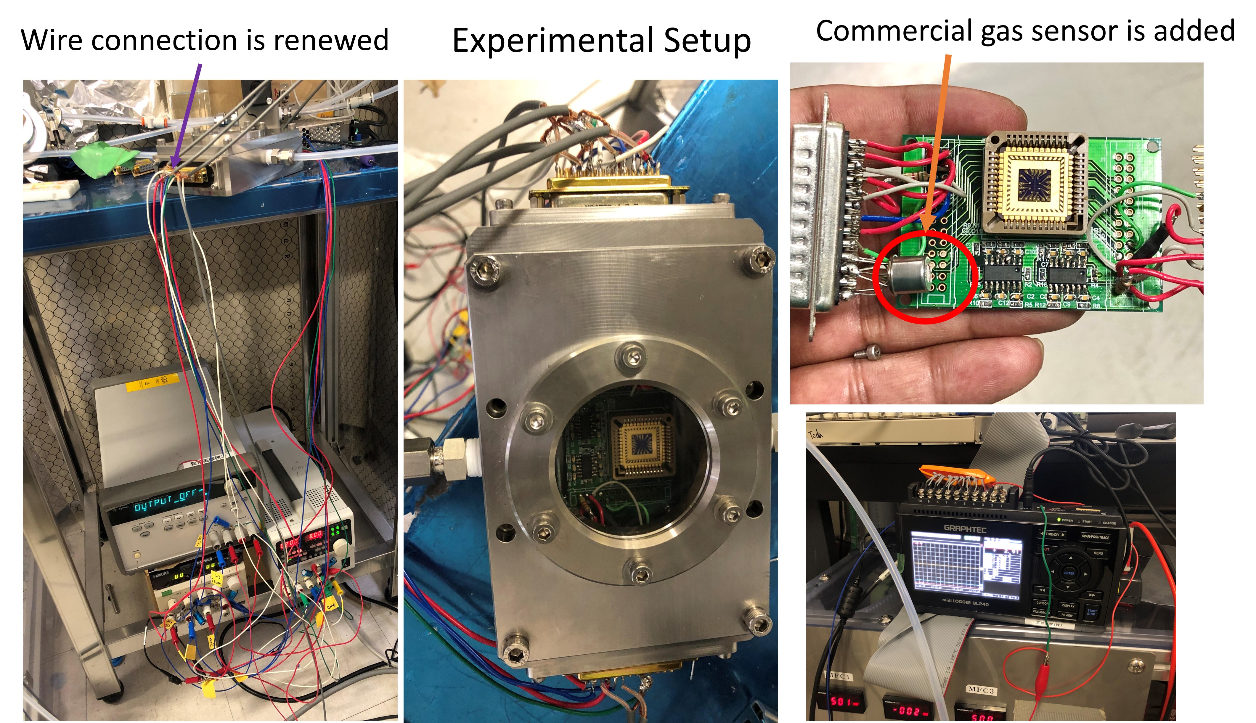
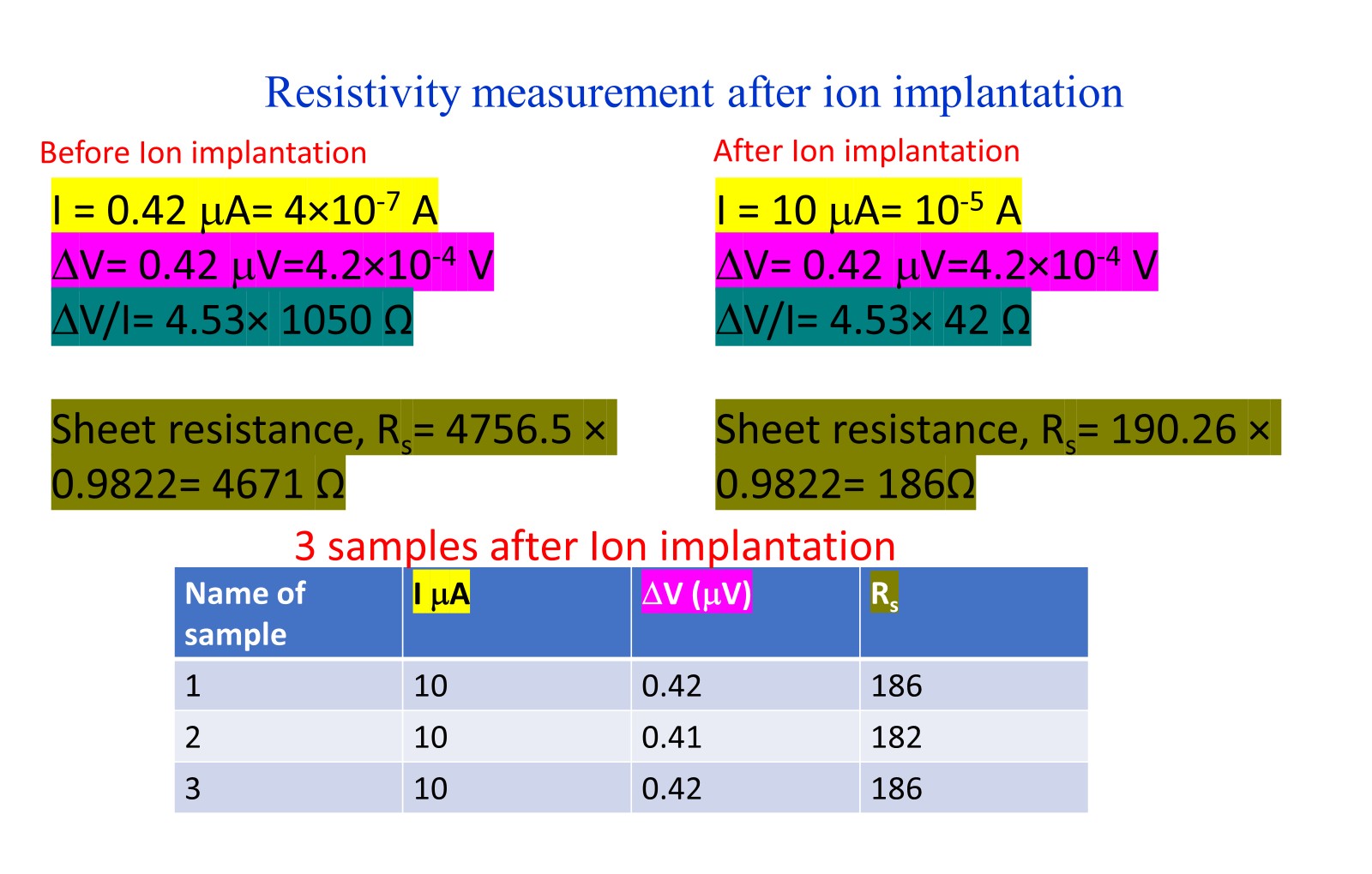
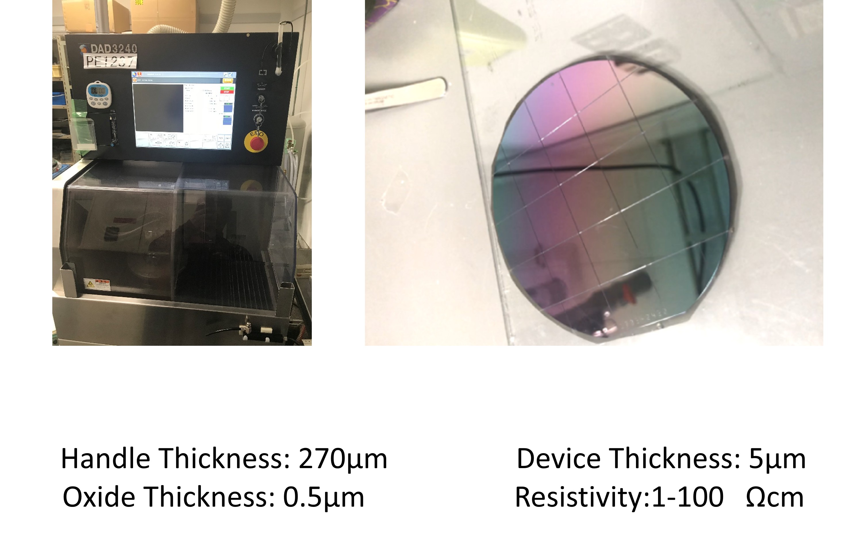
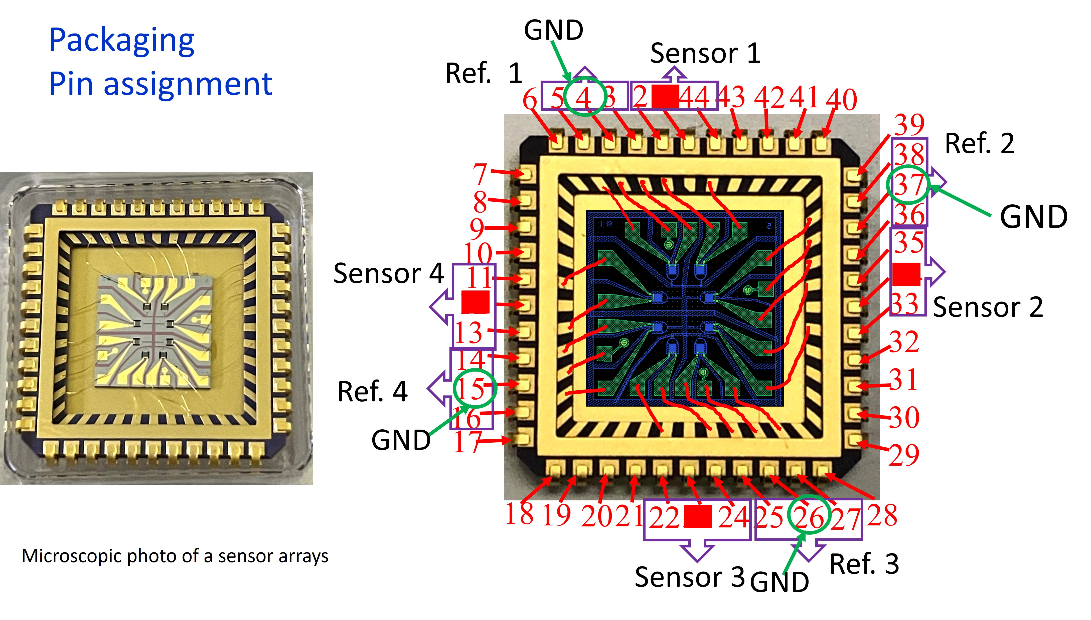
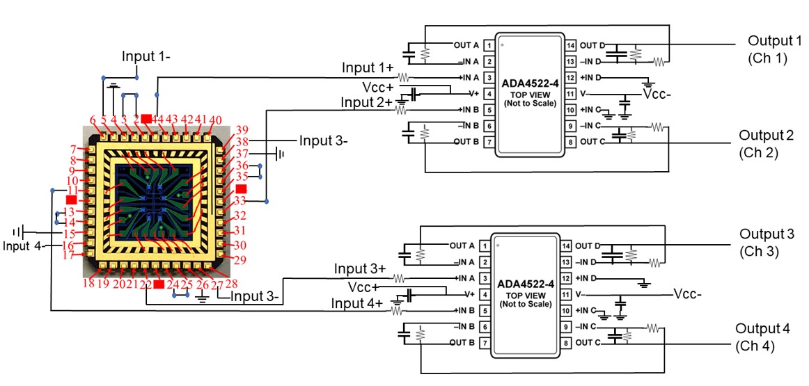
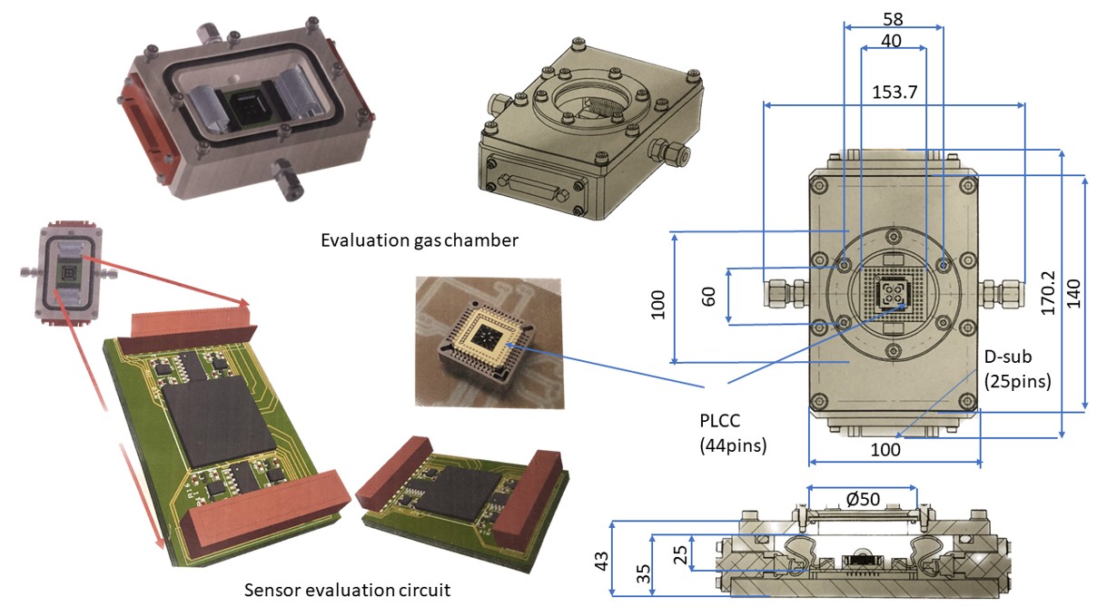
Following wafer dicing, the individual sensor die required meticulous packaging and electrical integration. This phase involved custom PCB design, wire bonding, and the development of signal acquisition circuitry to read out the piezoresistive changes induced by nanomechanical deflection. Concurrently, extensive metrology—including sheet resistance profiling and SEM inspection—was conducted to validate the electrical and physical parameters of the integrated module before environmental testing.
Final Gas Chamber Integration & Testing

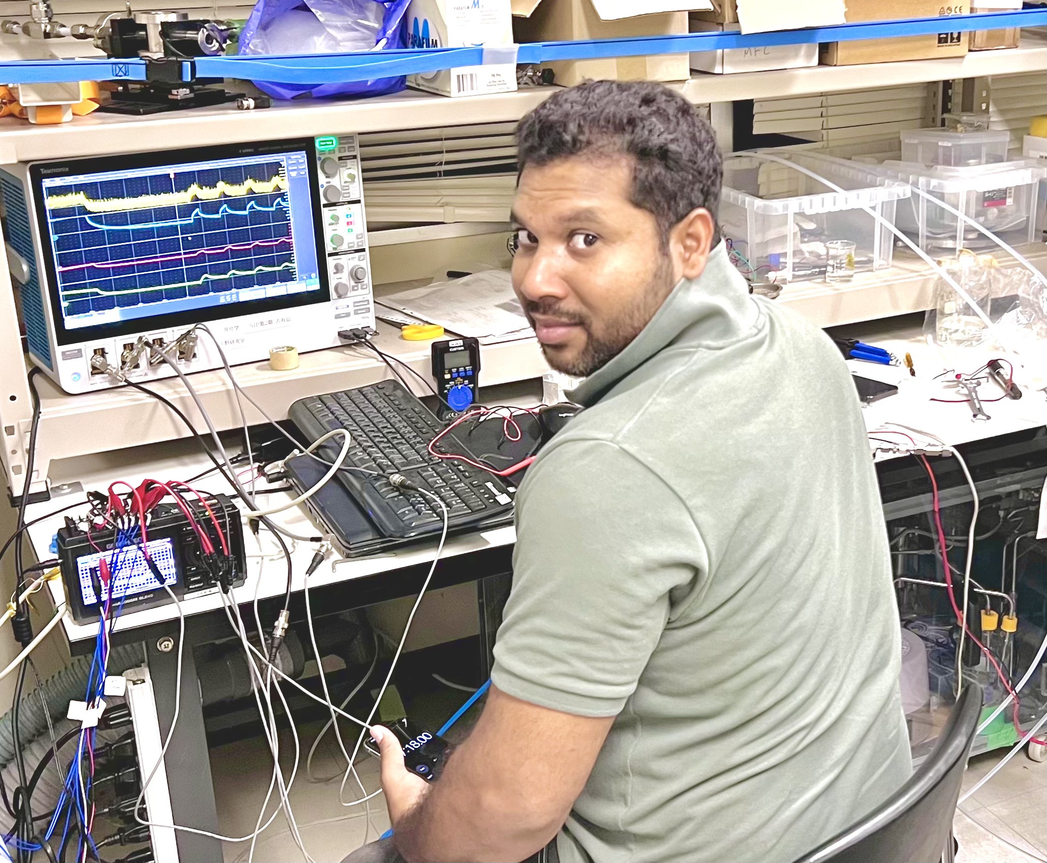
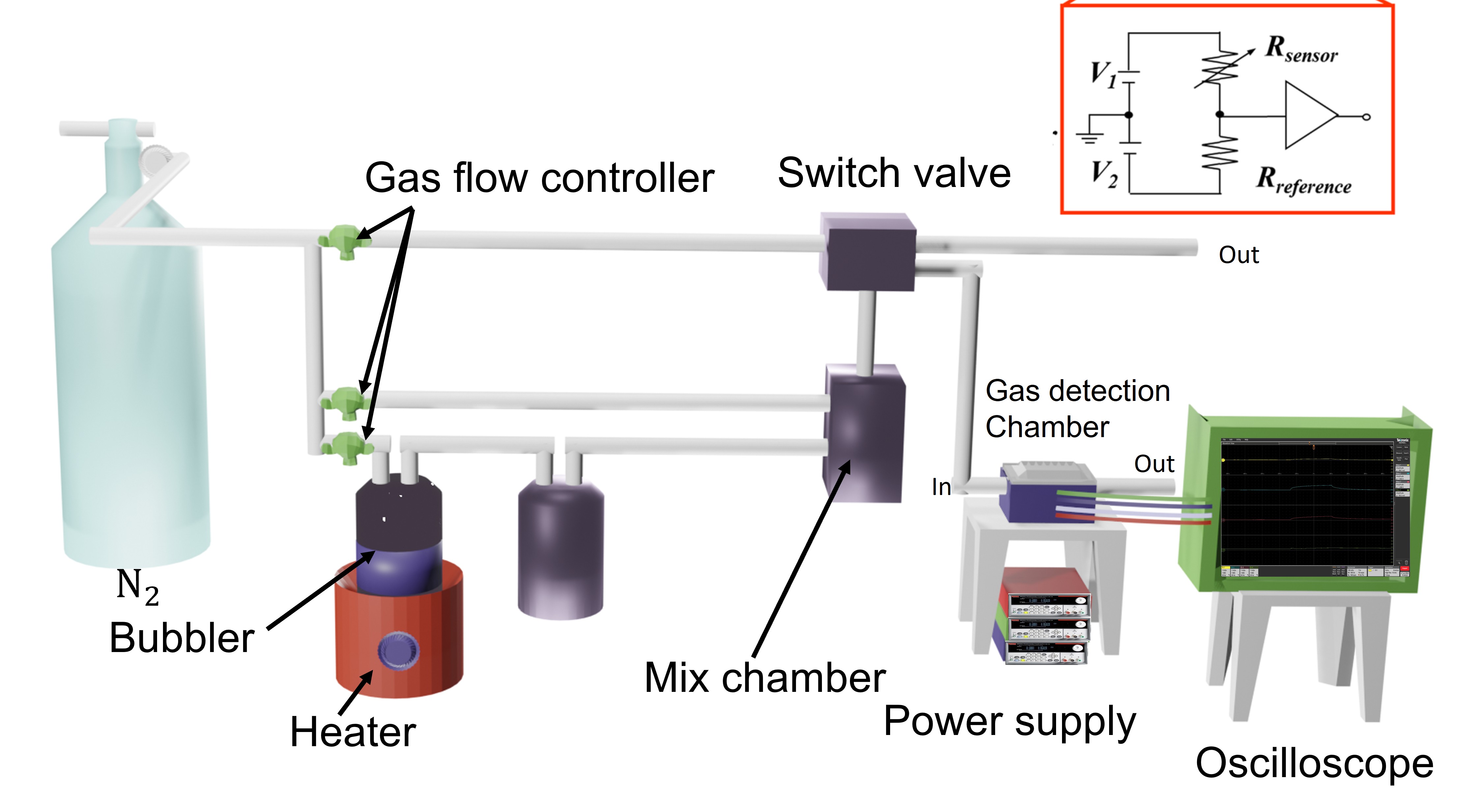
To empirically prove the sensing mechanism under real-world conditions, a custom, controlled-environment gas chamber was designed and assembled. Precise mass flow controllers were utilized to introduce specific concentrations of target volatile organic compounds (VOCs). The final assembled sensor chip demonstrated exceptional sensitivity and repeatability, validating the theoretical models and successfully meeting the commercial milestones defined by Mitsui Chemicals.
Prototype Fabrication, Packaging & Technology Transfer

Following successful process optimization and sensor validation, I transitioned the technology from wafer-level fabrication to fully packaged sensor prototypes suitable for external evaluation and commercialization activities.

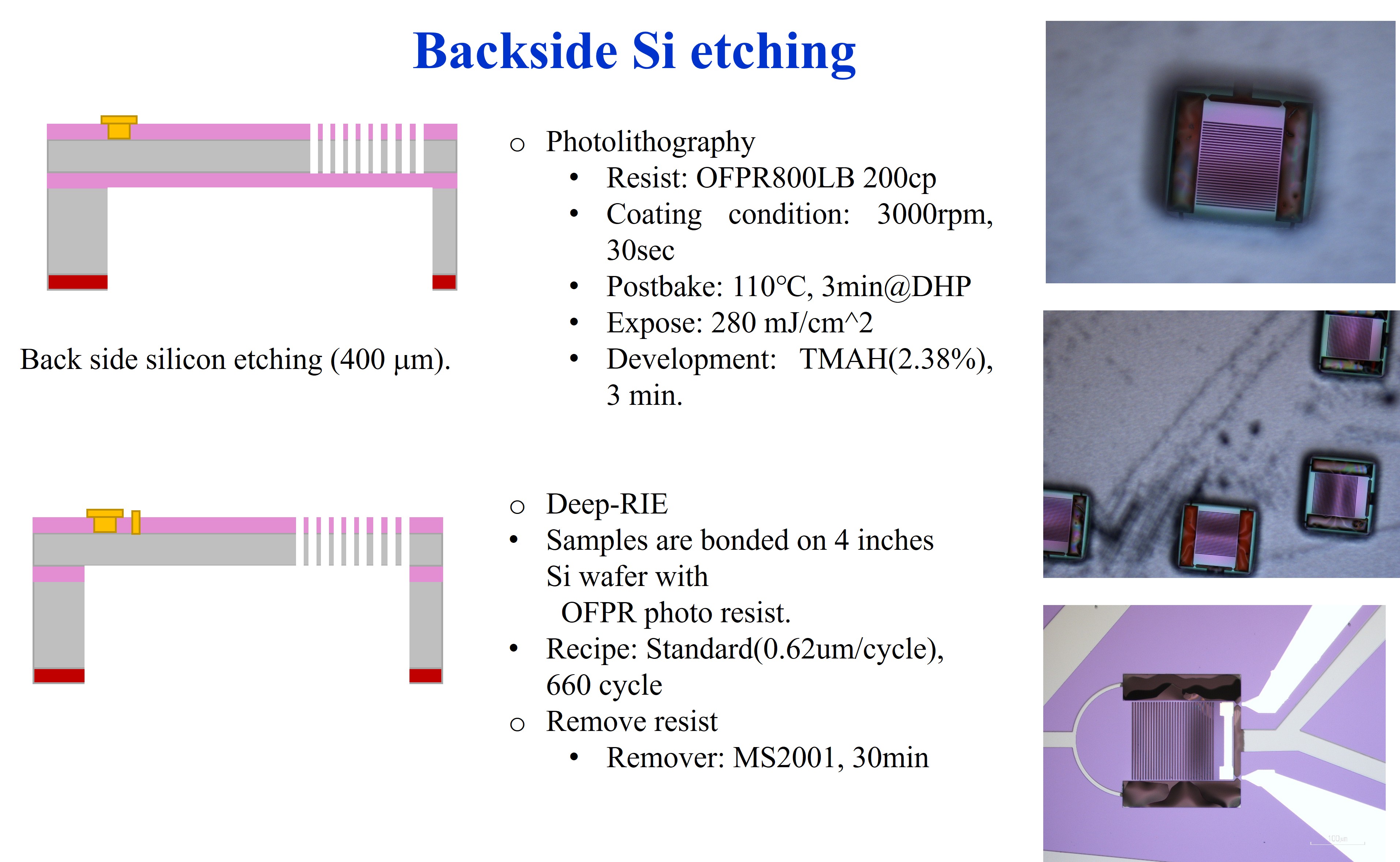
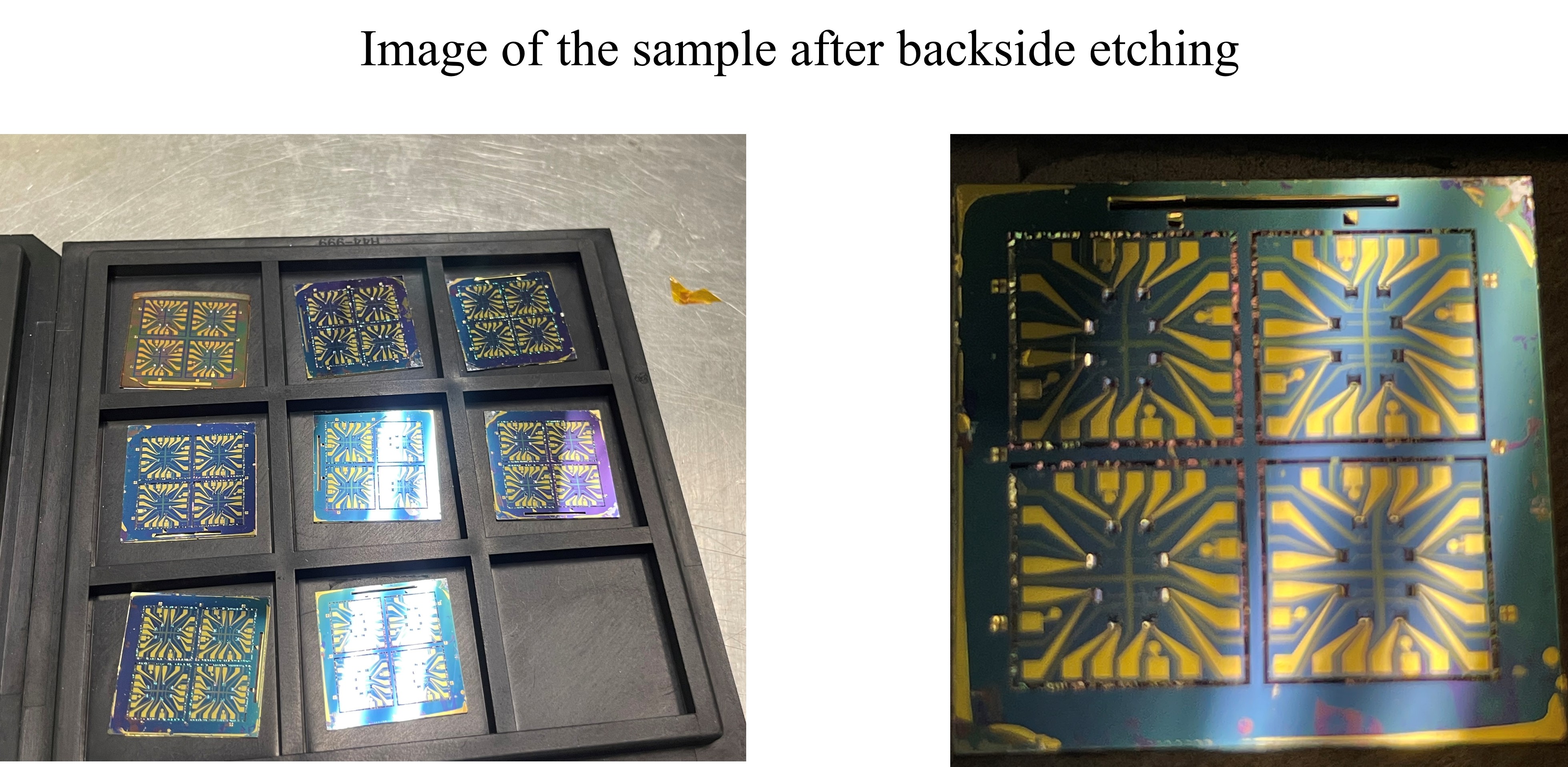
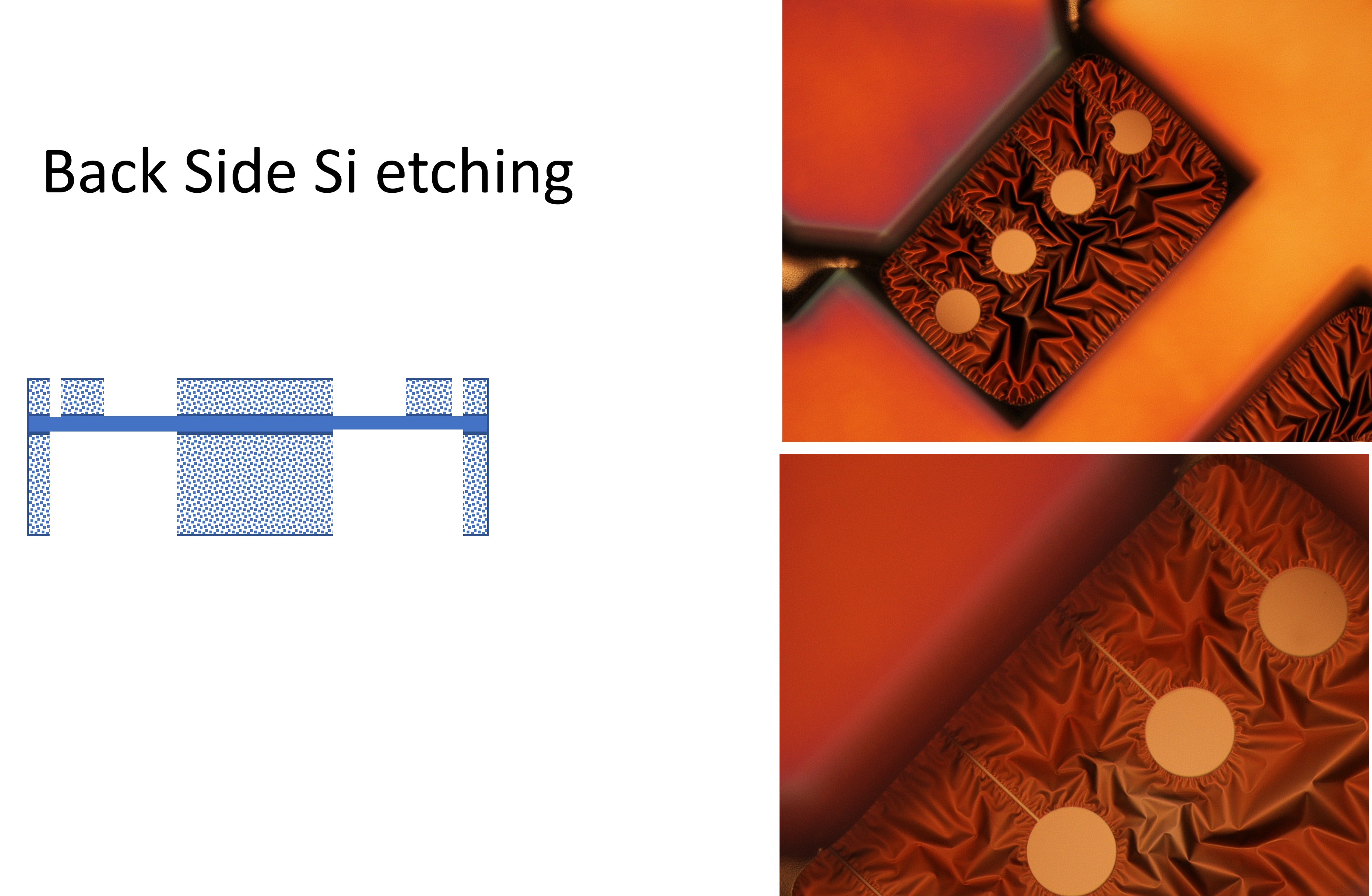
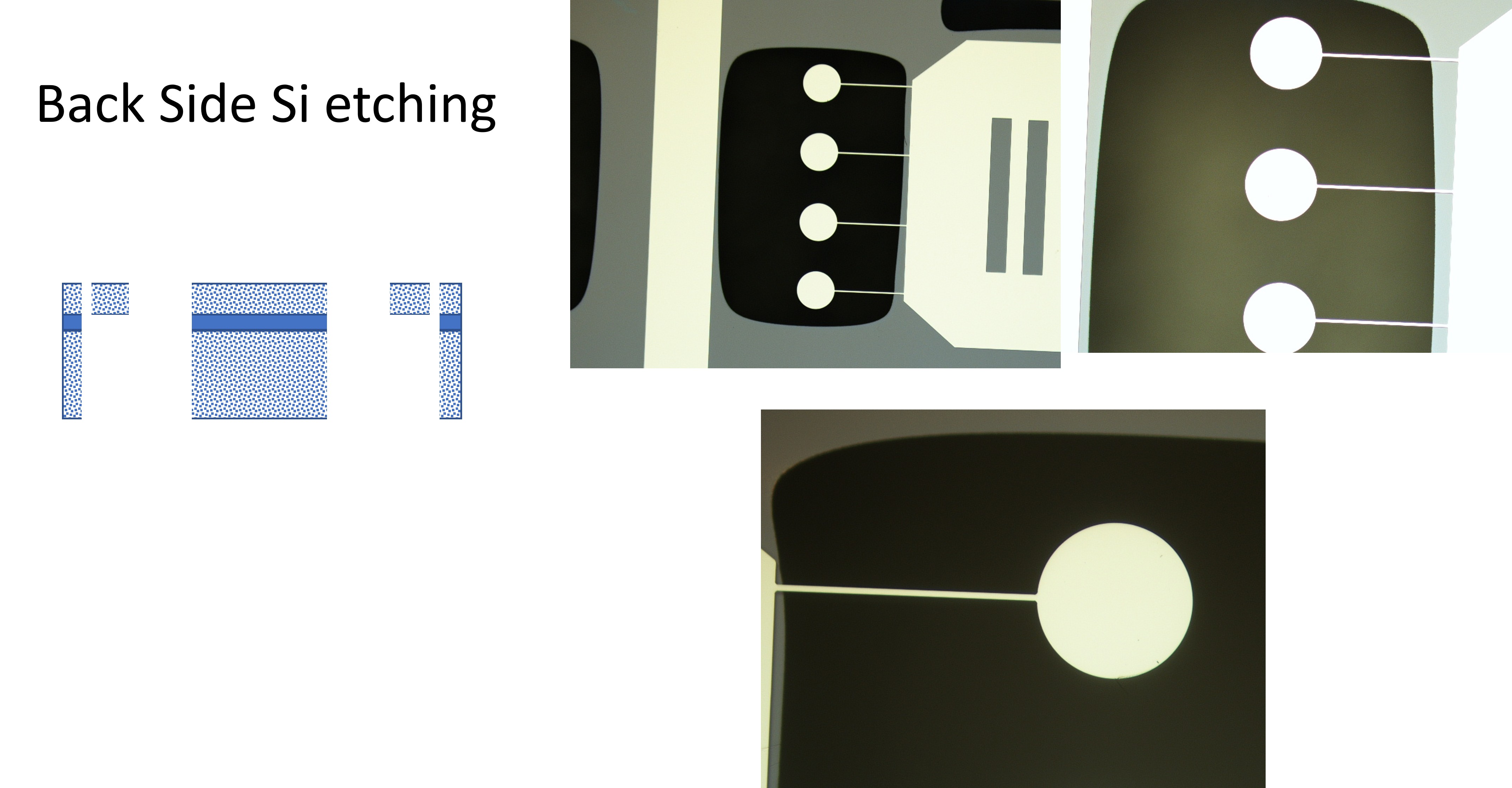
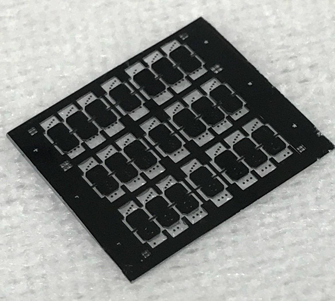
The fabricated wafers contained multiple nanomechanical sensor arrays, each integrating suspended silicon slit structures, piezoresistive transducers, and polymer-functionalized sensing regions. After completing backside silicon etching and structural release, the wafers were inspected to verify device integrity and fabrication yield.

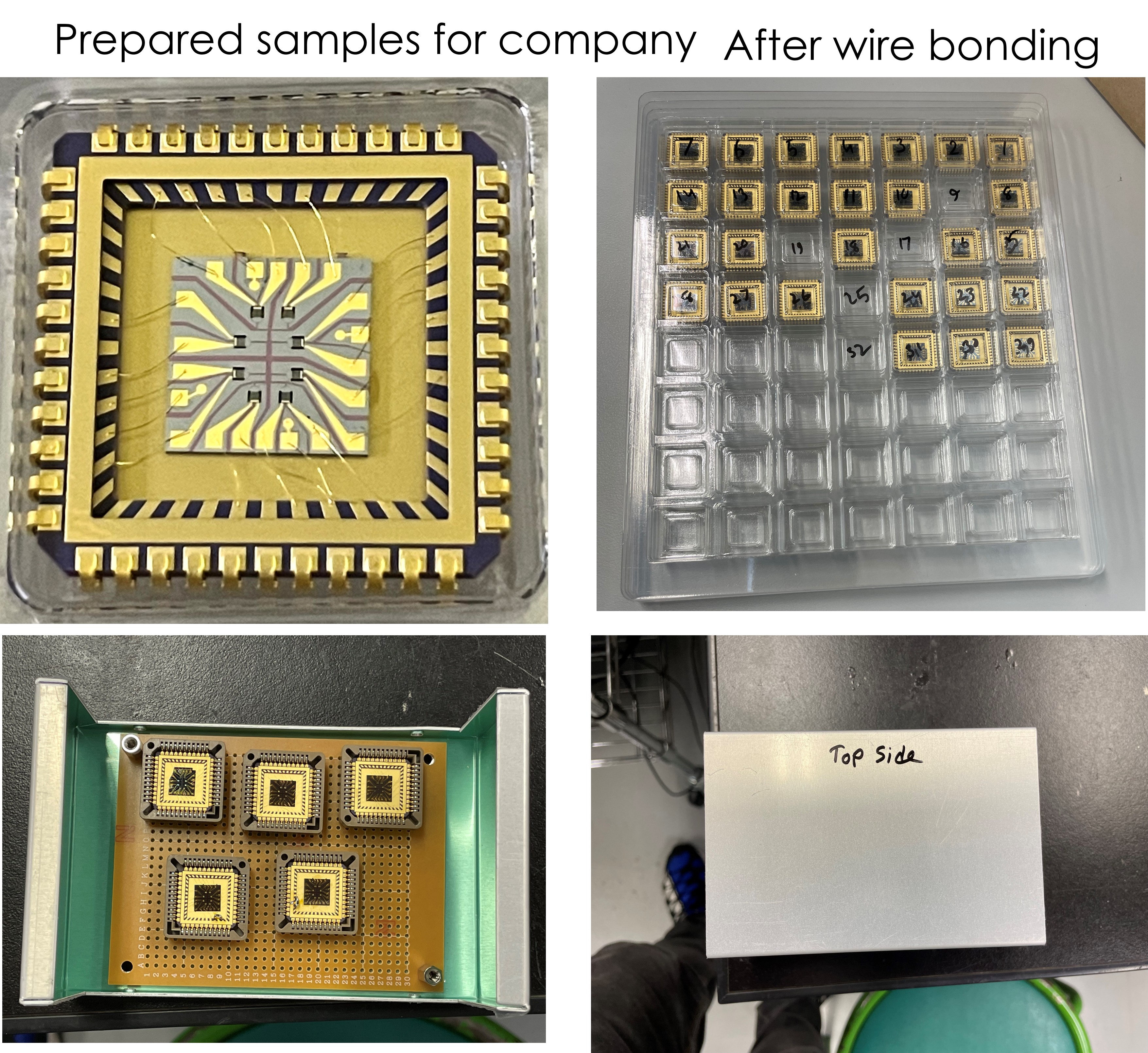
Individual sensor dies were then separated, packaged into ceramic PLCC carriers, and wire-bonded to establish reliable electrical connections between the MEMS device and external measurement electronics. Each packaged sensor underwent visual inspection, electrical continuity verification, and handling qualification before shipment.

To support industrial evaluation, I prepared multiple prototype batches with controlled documentation, labeling, packaging, and handling procedures. The final devices were delivered to Mitsui Chemicals for independent testing, performance verification, and commercialization assessment.

This phase required close coordination between fabrication, packaging, quality control, and industrial stakeholders to ensure that laboratory-scale devices could be reliably transferred into an industrial evaluation environment. The successful delivery of functional prototypes represented a critical milestone in advancing the technology from research development toward real-world deployment.
Videos

Watch the physical demonstration and the separation of a single nanomechanical gas sensor from the fabricated silicon wafer.

Publication & Media Impact

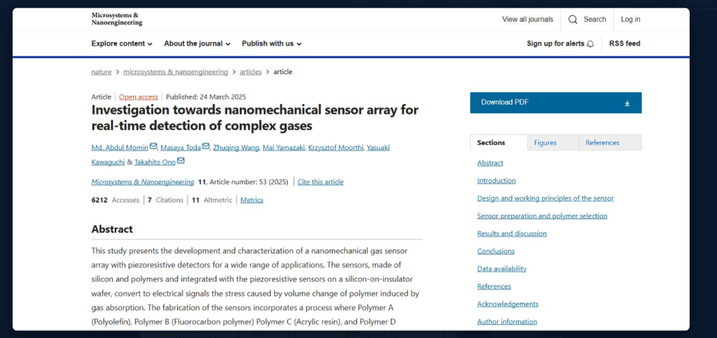
The successful optimization of this nanomechanical gas sensor not only met the scalability requirements for Mitsui Chemicals but also led to a high-impact publication in Nature's Microsystems & Nanoengineering . Due to its significant technological advancement, the research was also featured in major science news outlets, including Phys.org .
Metrology & Skills

  • SEM
  • ellipsometry
  • surface profilometry
  • optical microscopy
  • photolithography
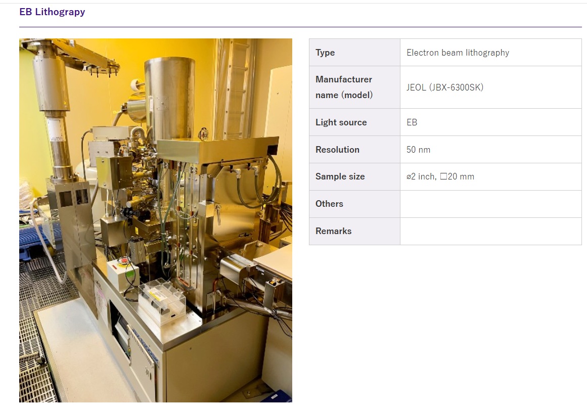
  • e-beam lithography
  • CVD
  • sputtering
  • ICP-RIE
  • device fabrication in cleanroom
  • process optimization
  • defect analysis
  • COMSOL simulation
  • ANSYS simulation
  • sensor performance evaluation
  • materials and geometry correlation
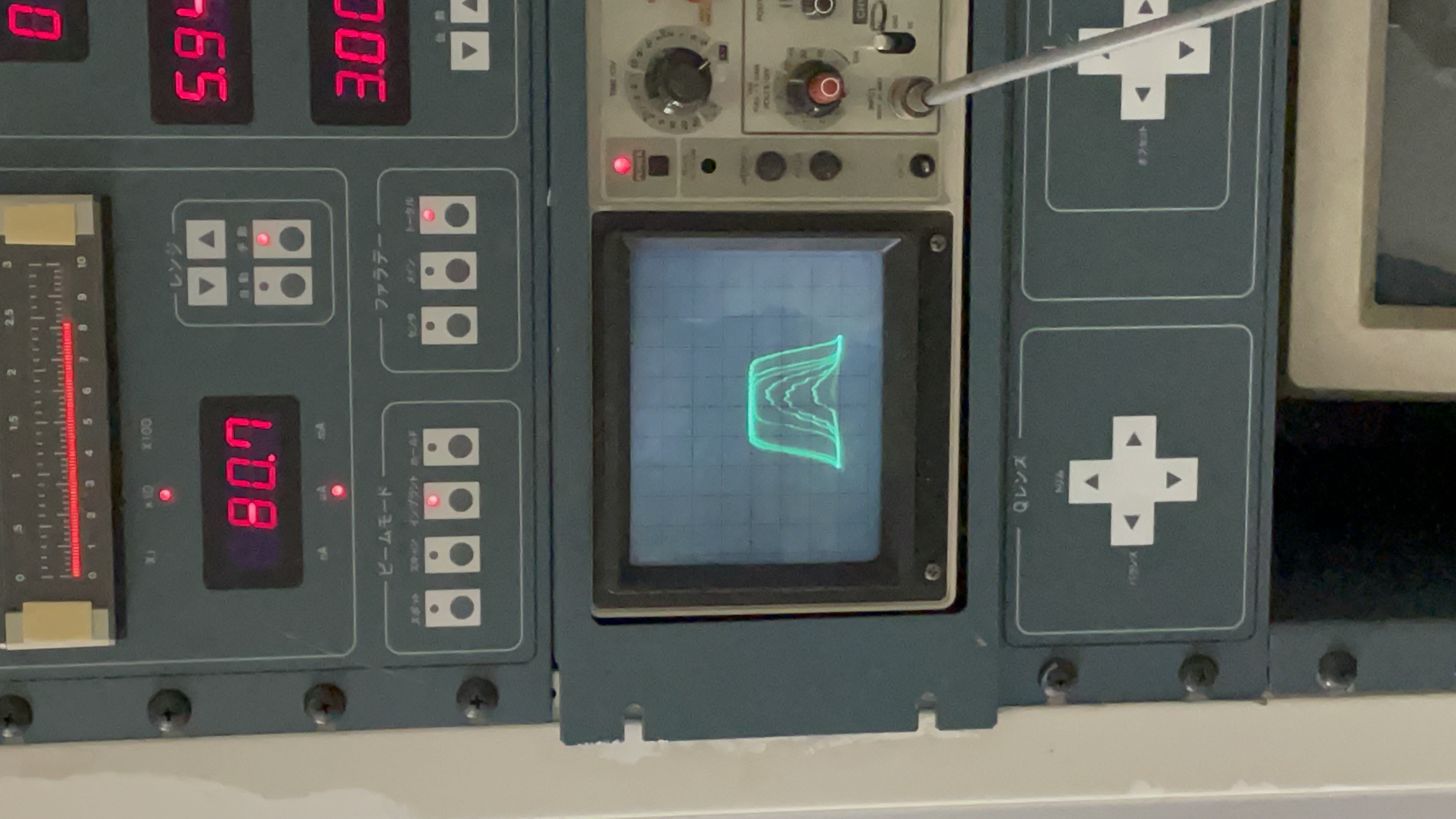
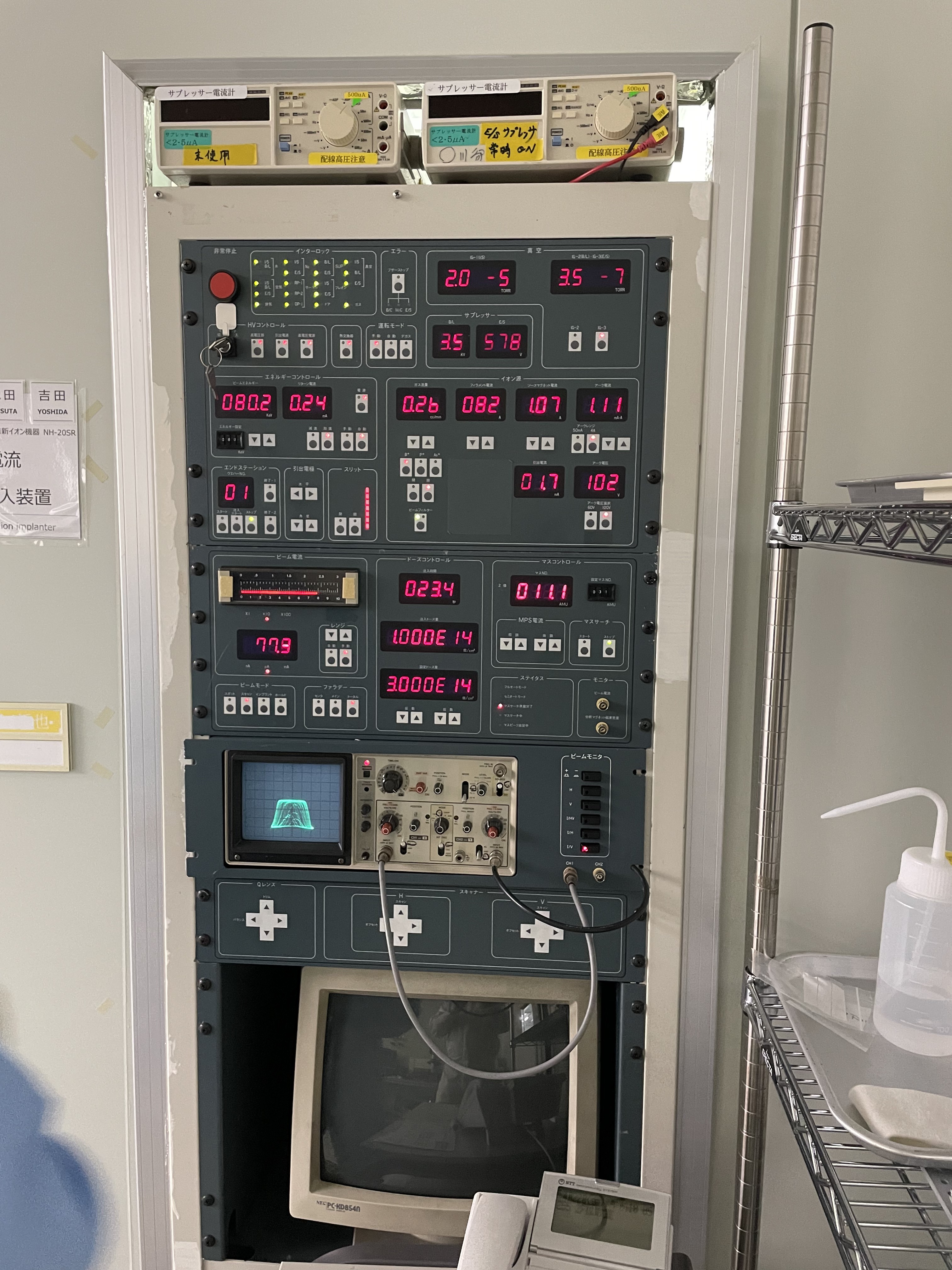
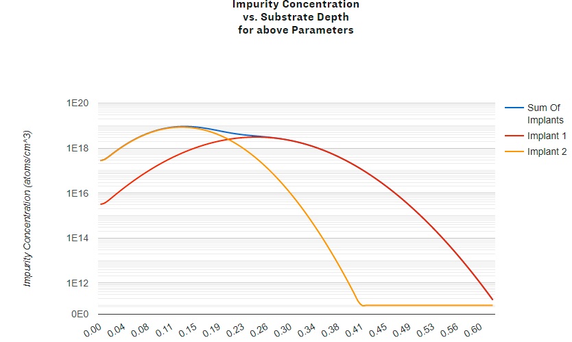
  • silicon conductivity improvement by boron doping
  • ion implantation and diffusion-related processing

Relevant Publications & Output

  1. Investigation towards nanomechanical sensor array for real-time detection of complex gases (Nature Microsystems & Nanoengineering)

Due to its significant technological advancement, the research was also featured in major science news outlets, including Phys.org.

Disclaimer: Some figures in this project story are taken from the relevant published journals referenced here, some are taken during the project while it was running (unpublished), and some are currently under review.
Fabrication of Silicon Cantilever-Based Nanomechanical Gas Sensor Array

Jump to published articles of this project

Project Overview

During this project, I developed a silicon-based nanomechanical cantilever gas sensor platform using semiconductor microfabrication technology. The goal was to fabricate a highly sensitive miniaturized sensor array capable of detecting different gas molecules by converting molecular interactions into mechanical deformation and electrical signals.

This project covered the complete semiconductor device development cycle — from mask layout design, wafer-level fabrication process development, process optimization, metrology characterization, device packaging, and sensor validation.

Cr Mask Design and Lithography Process Development

The first step of this project was the design of the complete photolithography mask set.

I designed the device layout using semiconductor layout design software and developed multiple Cr masks required for different fabrication layers.

The mask design included:

  • Cantilever structure geometry
  • Electrode patterns
  • Piezoresistor regions
  • Metal contact pads
  • Front-side device structures
  • Backside silicon release windows

A total of six Cr masks were designed and fabricated for the complete MEMS process flow.

After mask design:

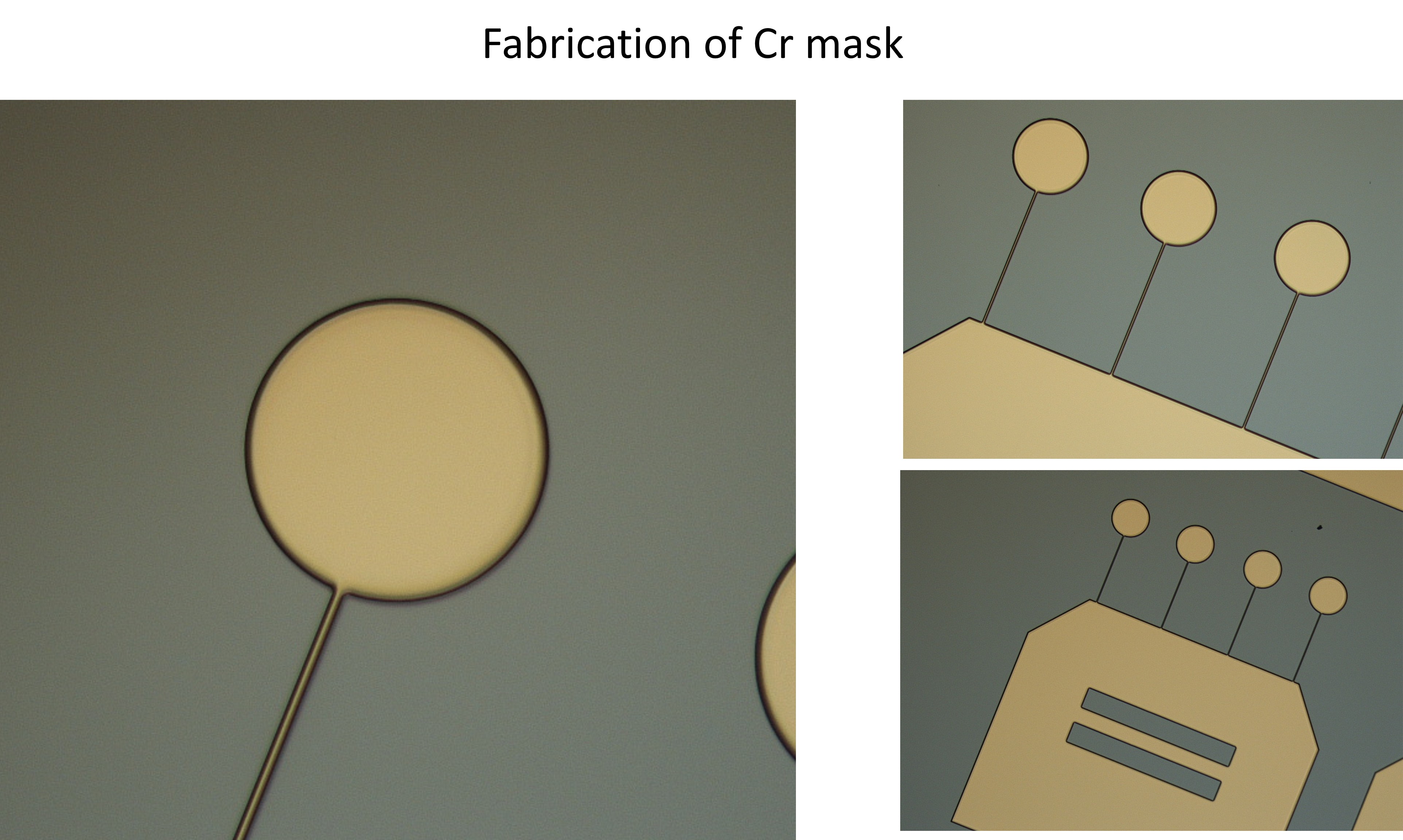
  • Laser lithography was used for pattern generation
  • Cr mask development was performed
  • Pattern dimensions and alignment accuracy were verified using optical microscopy

Critical dimensions including cantilever length, width, electrode spacing, and sensing regions were optimized to improve device sensitivity.

SOI Wafer-Based MEMS Fabrication

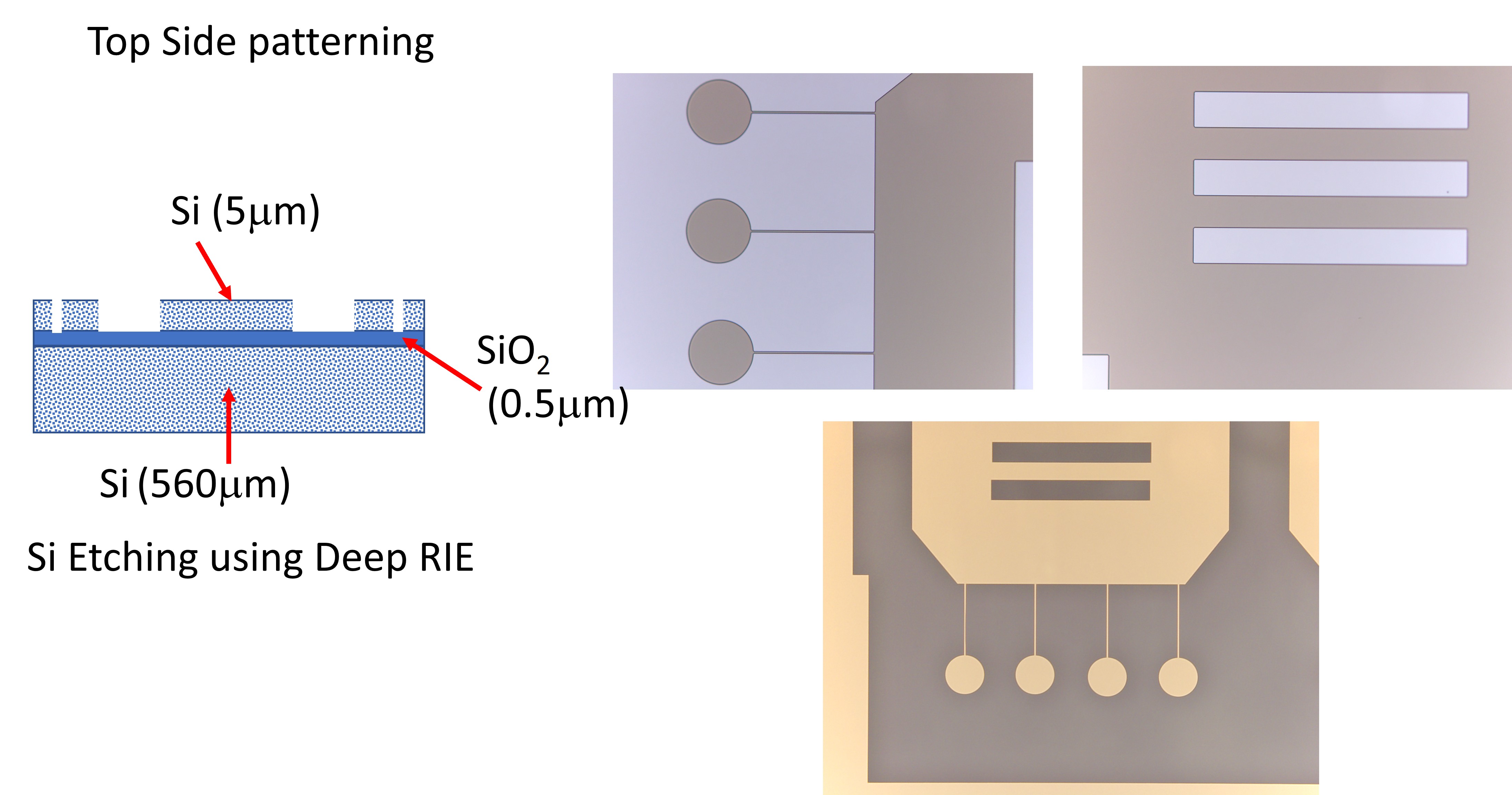
The sensor was fabricated using Silicon-On-Insulator (SOI) wafer technology to achieve precise control of the suspended silicon structure.

Starting substrate:

  • SOI wafer
  • Device Si layer: ~5 µm
  • Buried SiO₂ layer: ~0.5 µm
  • Handle Si layer: ~560 µm

The complete fabrication process included:

  1. Wafer cleaning and surface preparation
  2. Front-side lithography patterning
  3. Silicon device layer etching using Deep Reactive Ion Etching (DRIE)
  4. Piezoresistive sensing structure formation
  5. Thin film deposition and patterning
  6. Metal electrode fabrication
  7. Back-side lithography alignment
  8. Deep backside silicon etching
  9. Cantilever release process
  10. Final device inspection and packaging

Process Development and Optimization

A major challenge was achieving a reliable suspended cantilever structure without mechanical failure.

I optimized several semiconductor fabrication parameters:

Lithography Optimization

  • Exposure conditions
  • Development time
  • Pattern resolution
  • Mask alignment accuracy

Dry Etching Optimization

  • DRIE etching rate
  • Etching uniformity
  • Sidewall profile
  • Selectivity between Si and SiO₂

Structural Optimization

Different cantilever geometries were designed and tested to improve mechanical response.

Parameters optimized:

  • Cantilever dimensions
  • Thickness
  • Mechanical stiffness
  • Stress distribution
  • Deflection sensitivity

The objective was to maximize gas-induced mechanical response while maintaining device reliability.

Metrology and Characterization

Multiple semiconductor metrology techniques were used throughout development.

  • Optical Microscopy: Lithography inspection, pattern transfer verification, etching quality analysis, defect inspection
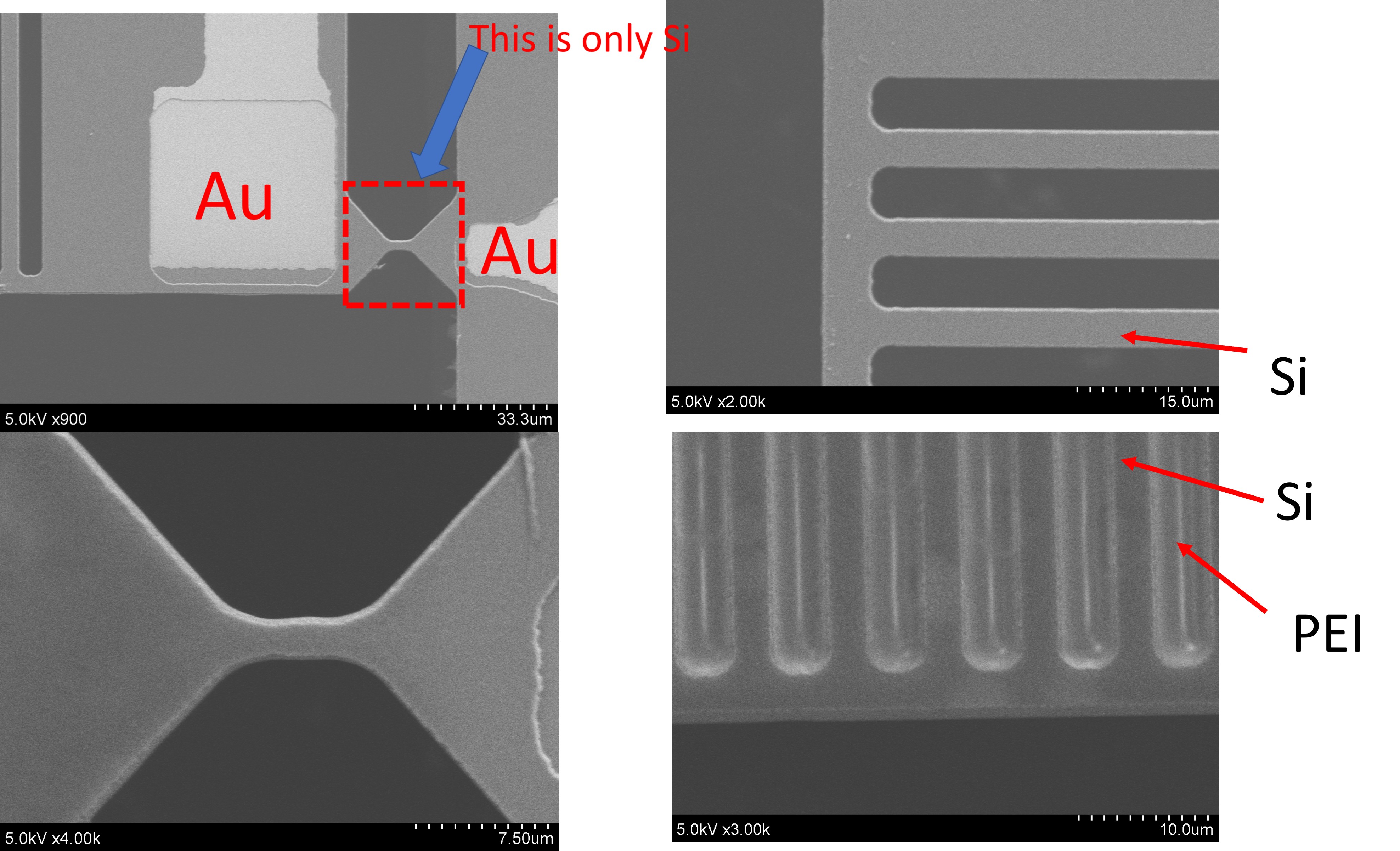
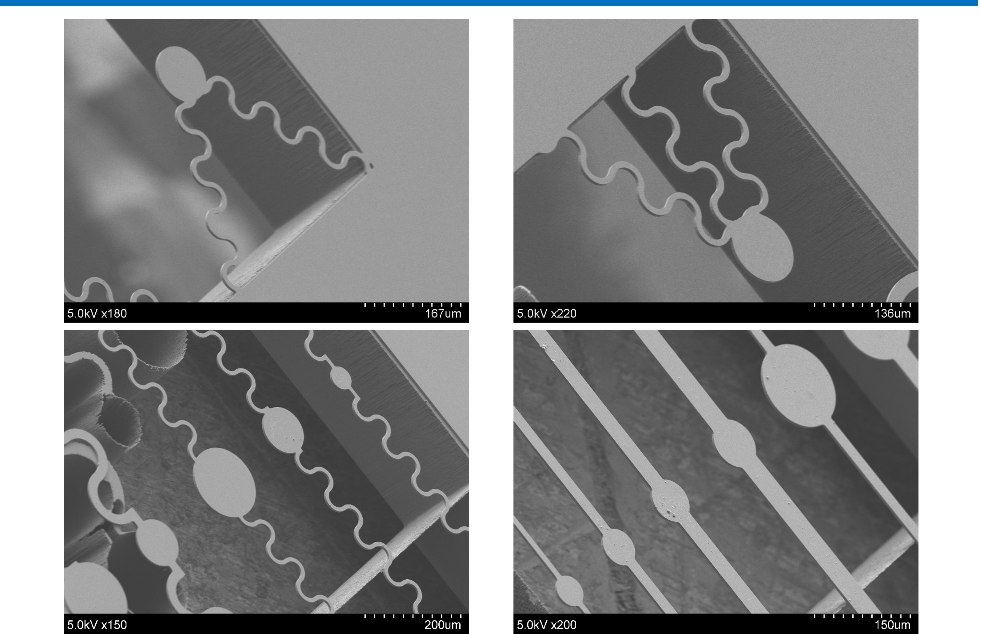
  • SEM Analysis: Microstructure verification, etched profile observation, released structure inspection
  • Electrical Characterization: Resistance measurement, piezoresistor performance evaluation, sensor response testing

Process Failure Analysis

Root cause analysis was performed to identify fabrication challenges including:

  • Over-etching
  • Incomplete silicon release
  • Pattern deformation
  • Mechanical stress-induced failure

Fabrication parameters were modified based on metrology feedback.

Metrology SEM

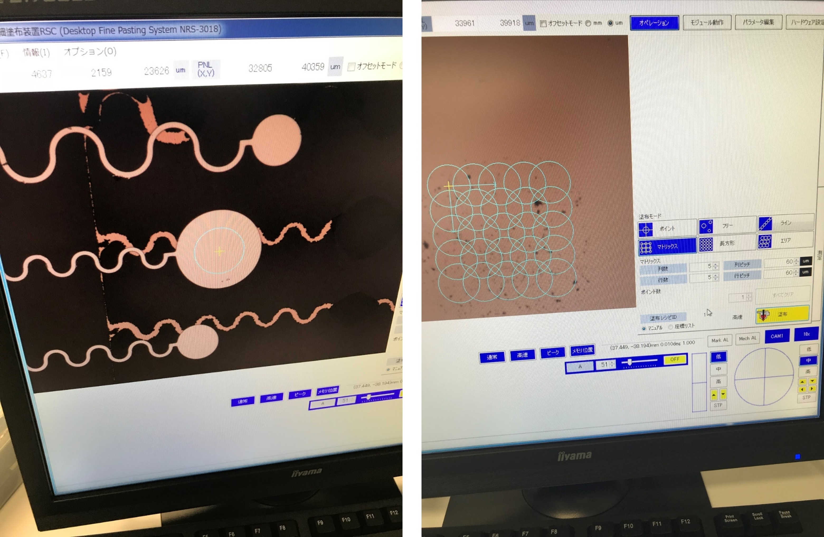
Polymer Deposition on Cantilever

Device Packaging and System Integration

After successful fabrication:

  • Individual sensor chips were diced
  • Devices were packaged
  • Wire bonding was performed
  • Electrical connection reliability was verified

The completed sensor chips were integrated into testing platforms for gas sensing experiments.

Engineering Impact

This project demonstrated my ability to develop a complete semiconductor MEMS device from concept to working prototype.

Key expertise developed:

Semiconductor layout design Cr mask fabrication Laser lithography Photolithography optimization SOI wafer processing DRIE silicon micromachining Thin-film process integration MEMS device fabrication Process troubleshooting Failure/root-cause analysis Device packaging and validation

This work represents a full semiconductor product development workflow:
Design → Mask Fabrication → Wafer Processing → Metrology → Optimization → Packaging → Functional Device

Disclaimer: Some figures in this project story are taken from the relevant published journals referenced here, some are taken during the project while it was running (unpublished), and some are currently under review.
Organic Solar Cell Process Development, Optimization & Reliability Engineering

Jump to published articles of this project
Project Focus: Semiconductor Process Engineering | Thin Film Device Fabrication | DOE Optimization | Root Cause Analysis

This project focused on developing high-performance organic photovoltaic (OPV) devices through systematic process engineering, device architecture optimization, and reliability investigation. The work followed an industry-style semiconductor development approach: design → fabrication → characterization → failure analysis → process improvement.

1. Device Architecture Development & Process Optimization

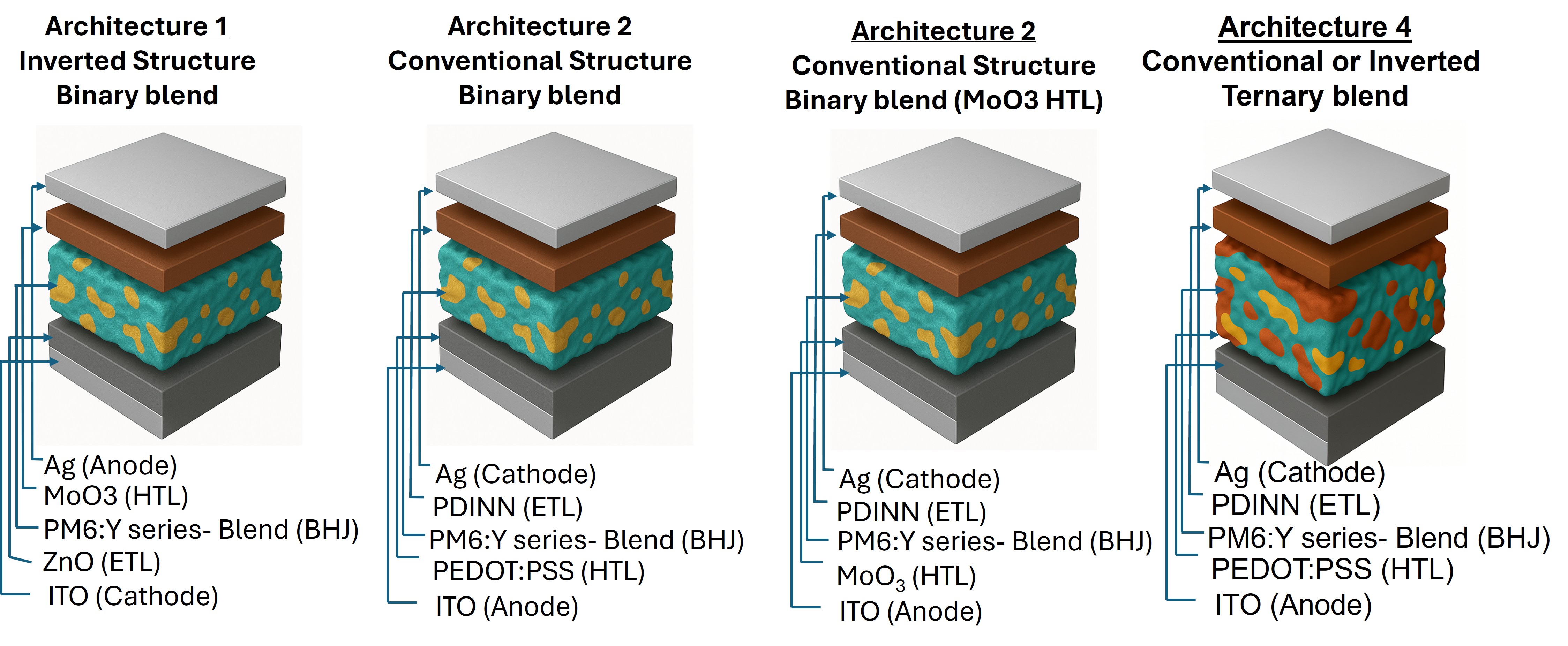
I developed and optimized multiple organic solar cell device architectures, including inverted and conventional structures with binary and ternary donor–acceptor blends.

Device stacks included:

  • Transparent conductive oxide substrates
  • Electron transport layers
  • Donor-Acceptor bulk heterojunction active layers
  • Hole transport layers
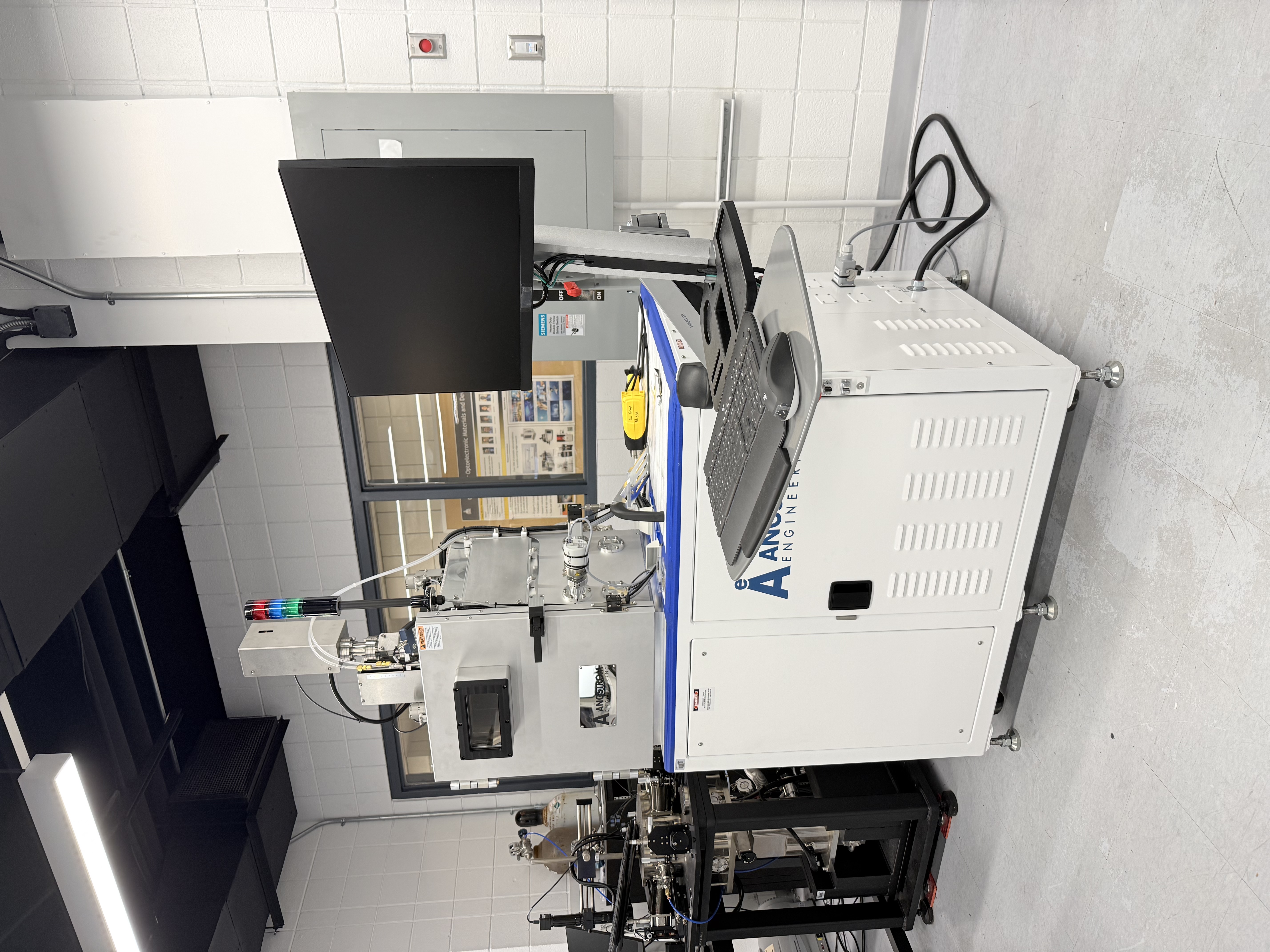
  • Thermally evaporated metal electrodes

Different donor/acceptor materials, blend ratios, layer thicknesses, processing conditions, and interface layers were optimized to maximize power conversion efficiency (PCE), reproducibility, and device stability.

2. High-Throughput Fabrication & DOE-Based Process Development

A Design of Experiments (DOE) strategy was implemented to understand the relationship between fabrication parameters and final device performance.

Process variables investigated:

  • Active layer concentration
  • Donor/acceptor ratio
  • Additive concentration
  • Spin coating speed
  • Annealing temperature
  • Annealing time
  • HTL/ETL thickness optimization

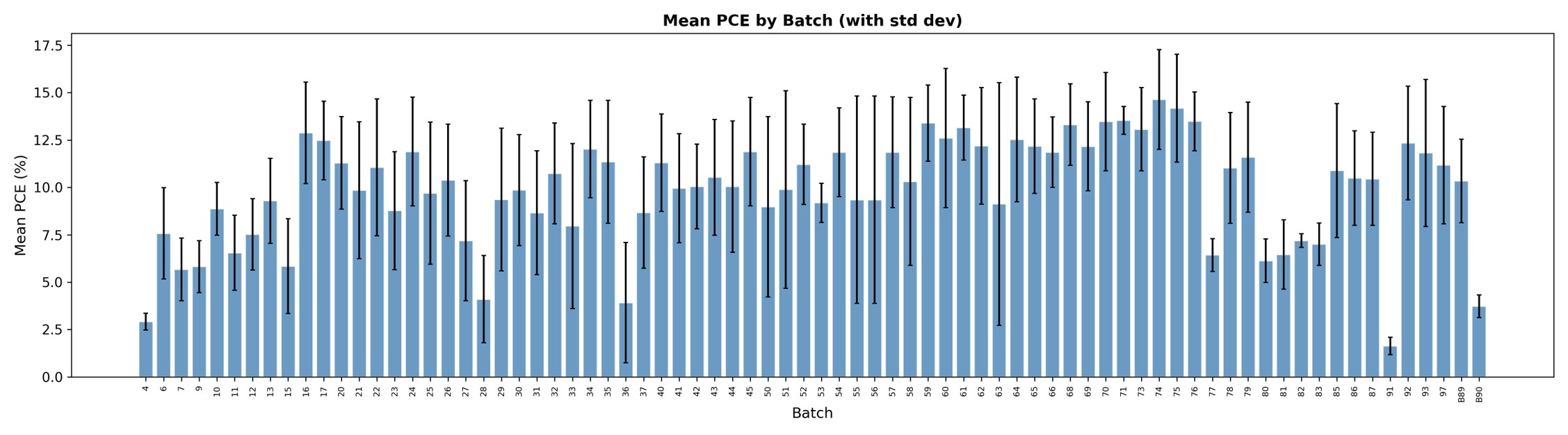
Fabricated more than 100 experimental batches. Each batch contained 12–20 substrates (20 mm × 20 mm), with each substrate integrating 8 individual solar cells. Large-scale fabrication statistics enabled identification of process windows, yield improvement strategies, and reproducible high-efficiency conditions.

3. Data-Driven Process Correlation Analysis

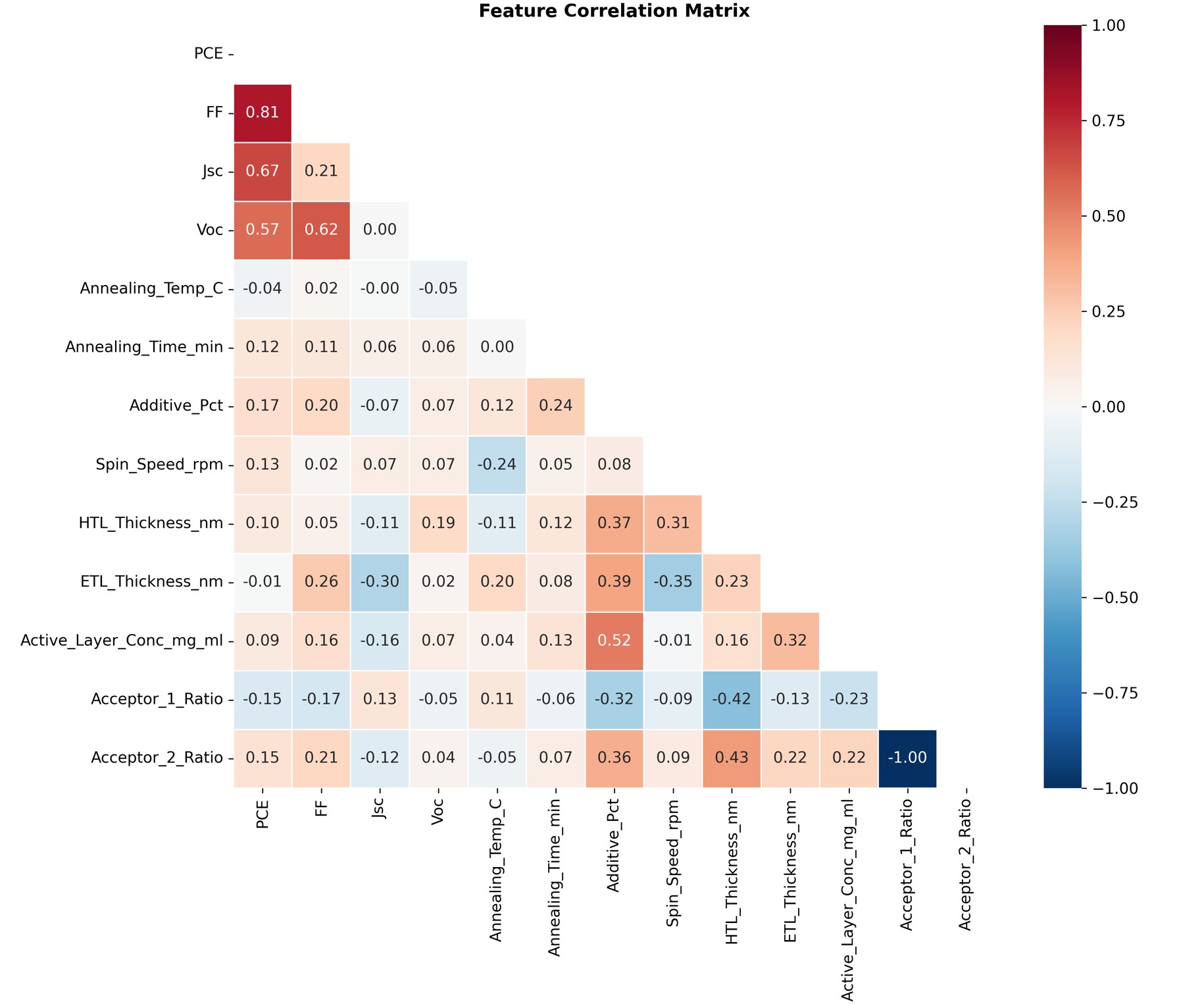
A process–performance correlation framework was developed to identify the dominant parameters controlling device efficiency.

Statistical analysis was performed between fabrication variables and photovoltaic parameters:

  • Power Conversion Efficiency (PCE)
  • Fill Factor (FF)
  • Short-circuit current density (Jsc)
  • Open-circuit voltage (Voc)

Correlation analysis revealed critical process contributors and guided further optimization of device fabrication conditions.

4. Reliability Testing & Root Cause Analysis of Degradation Pathways

Long-term thermal stability experiments were performed by monitoring device performance degradation over time. When performance degradation was observed, a semiconductor-style root cause analysis workflow was applied:

Problem: Device efficiency and stability decreased after thermal aging.

Investigation: Advanced thin-film metrology was used to analyze degradation mechanisms:

  • Active layer morphology evolution
  • Interface degradation
  • Film uniformity changes
  • Material redistribution and phase separation

Root Cause Analysis: The degradation pathway was identified by correlating electrical performance loss with physical and material changes in the device stack.

Solution Strategy: Processing conditions and device structures were optimized to improve morphology stability, device lifetime, and fabrication reproducibility.

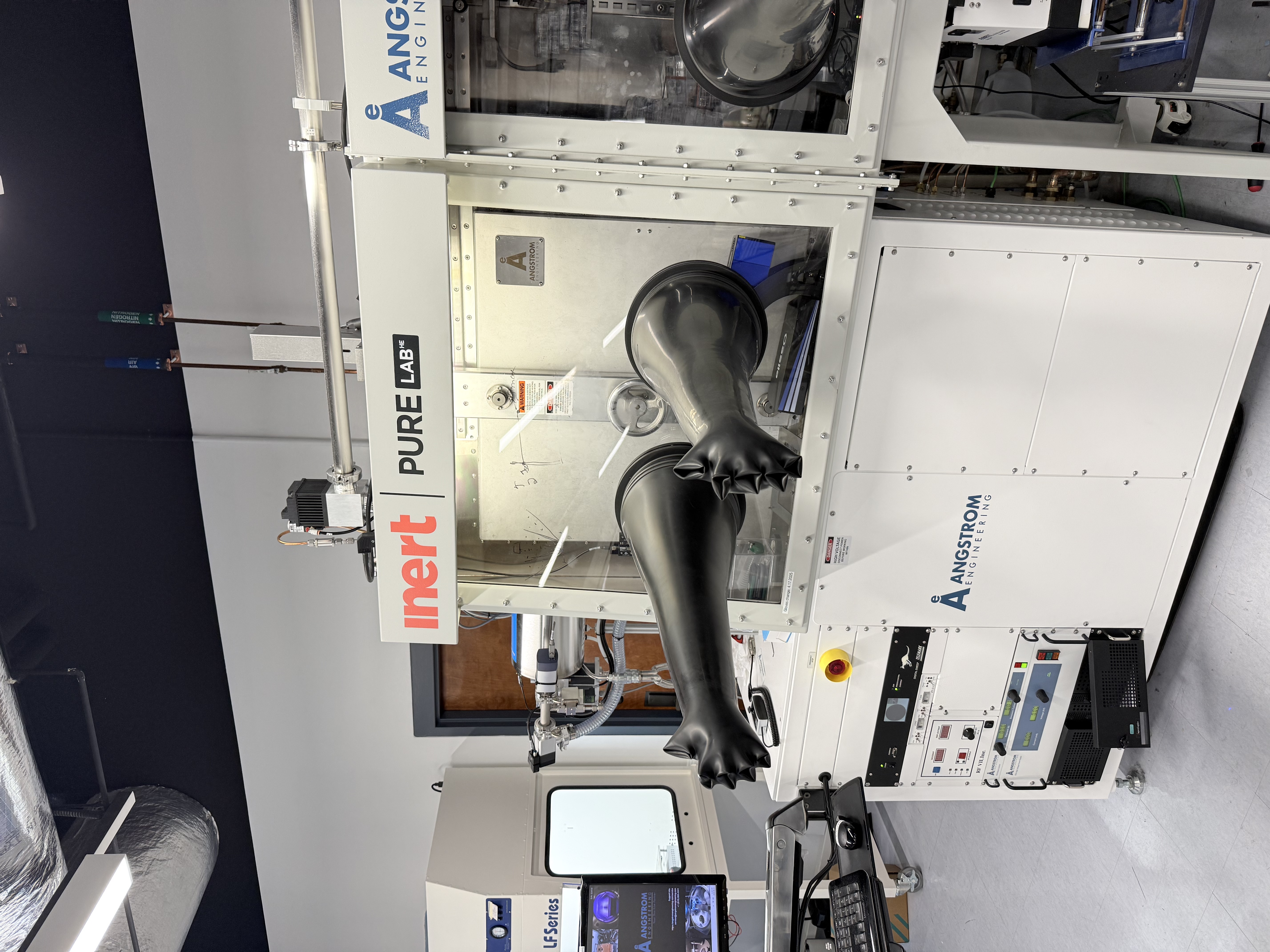
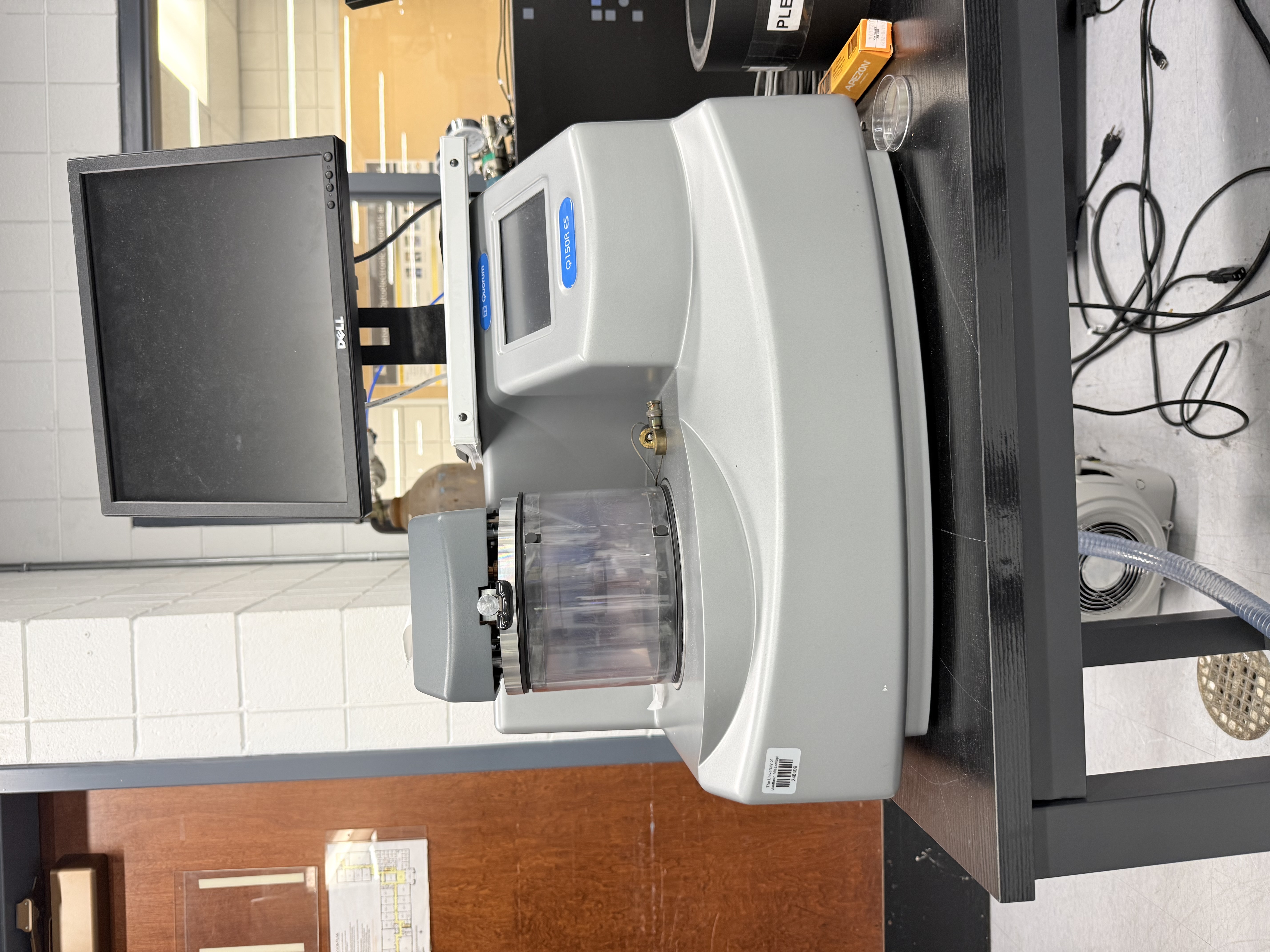
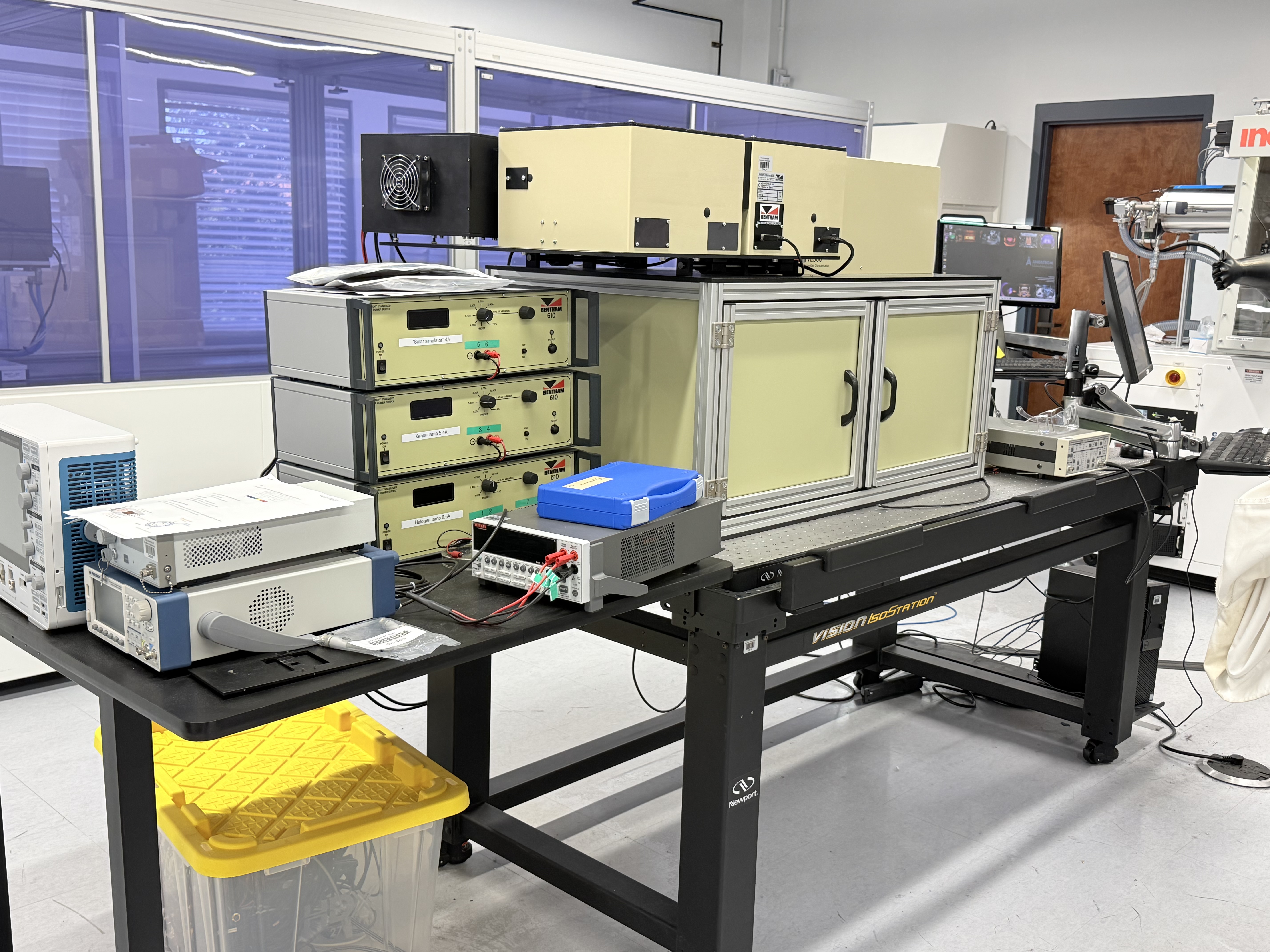
Instrumentation & Metrology

5. Semiconductor Manufacturing Relevance

This project directly connects with semiconductor and thin-film manufacturing workflows:

  • Thin-film deposition process optimization
  • DOE-based process development
  • Device fabrication and yield improvement
  • Failure analysis and troubleshooting
  • Materials characterization and reliability engineering
  • Data-driven process control

The approach follows industrial engineering methodology used in semiconductor, display, photovoltaic, and advanced device manufacturing.

Research Output

Based on this work, three peer-reviewed manuscripts are currently in preparation:

  1. Process optimization and performance enhancement of organic solar cells
  2. Thermal reliability testing and degradation mechanism analysis
  3. Morphology-driven structure–property relationship and failure pathway investigation

Metrology & Skills

  • J-V characterization
  • EQE / spectral response
  • UV-Vis spectroscopy
  • GIWAXS
  • AFM-IR
  • SEM
  • profilometry / thickness measurement
  • DSC
  • Flash-DSC
  • thermal aging studies
  • humidity stability testing
  • degradation analysis
  • device performance correlation
  • Python data analysis
  • materials / interface optimization

Relevant Publications & Output

Based on this work, the following outputs have been produced:

  1. Md Abdul Momin et al., Understanding Molecular Architecture of Non-Fullerene Acceptors: Impacts on Crystallization Kinetics and Thermal Stability... ACS National Meeting 2026 (Atlanta, GA)
  2. Md Abdul Momin, Mona Gulied, Andrew Bates, Guillaume Freychet, Xiaodan Gu* Understanding Molecular Architecture of Non-Fullerene Acceptors: Impacts on Crystallization Kinetics and Thermal Stability in Organic Solar Cells. Will be submitted soon.....

Disclaimer: Some figures in this project story are taken from the relevant published journals referenced here, some are taken during the project while it was running (unpublished), and some are currently under review.
Plasma Polymerized Thin Film Development: Material Design, PECVD Process Optimization & Device Characterization

Jump to published articles of this project

Project Overview

Developed plasma-polymerized thin films through a complete semiconductor process development workflow including material selection, PECVD deposition, DOE optimization, advanced metrology, root cause analysis, and electrical/optical reliability validation.

The complete development strategy:
Material Design → Plasma Process Development → Thin Film Fabrication → Metrology Characterization → DOE Optimization → Reliable Device Integration

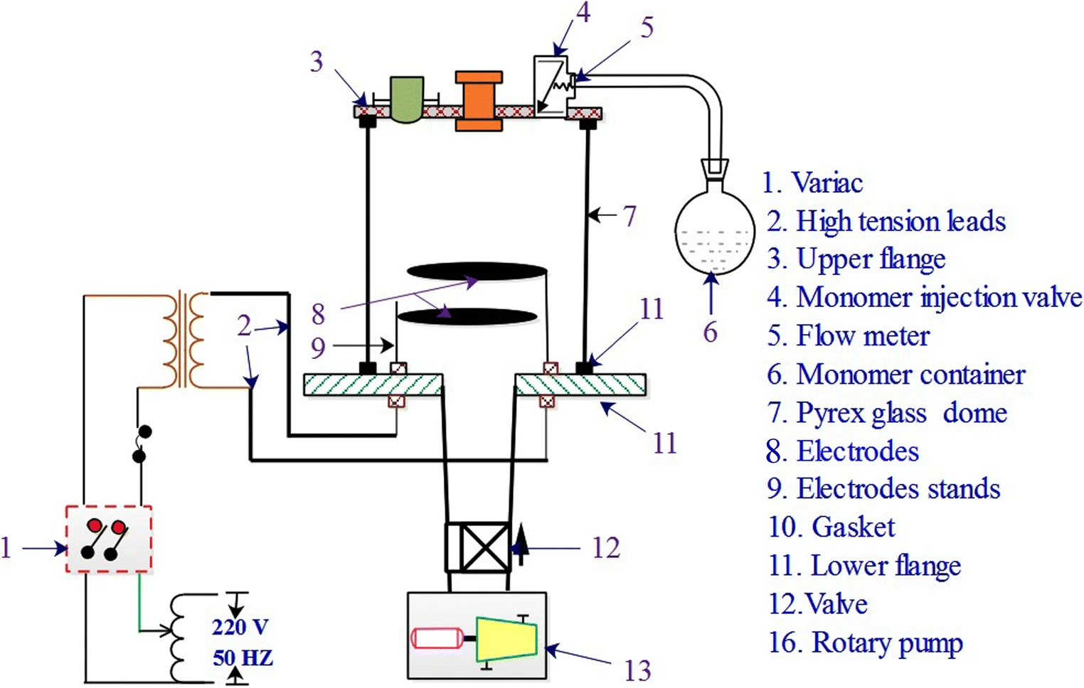
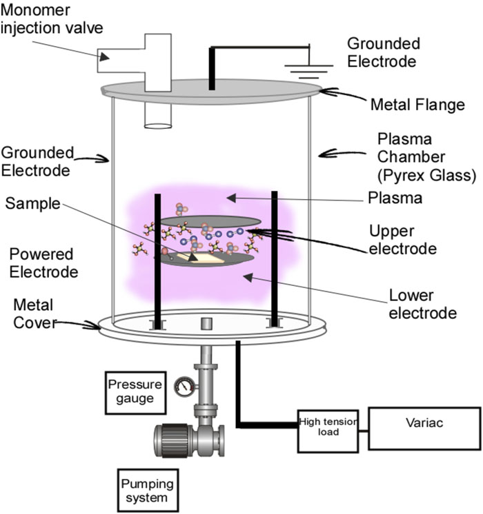
1. Custom PECVD System Development & Thin Film Fabrication

A custom PECVD system was developed for plasma polymer thin-film fabrication.

Major work:

  • Designed experimental plasma deposition setup
  • Controlled plasma polymerization process
  • Optimized deposition parameters
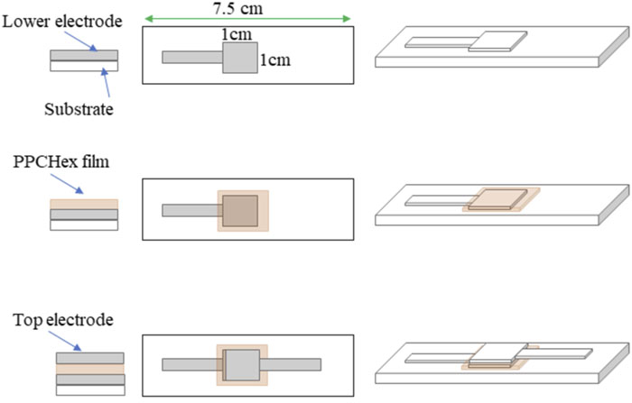
  • Fabricated metal–insulator–metal structures for electrical characterization

2. Material Selection, Computational Study & DOE Optimization

Different precursor materials were selected and investigated using a material engineering approach.

Performed:

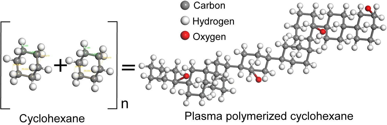
  • Molecular structure analysis
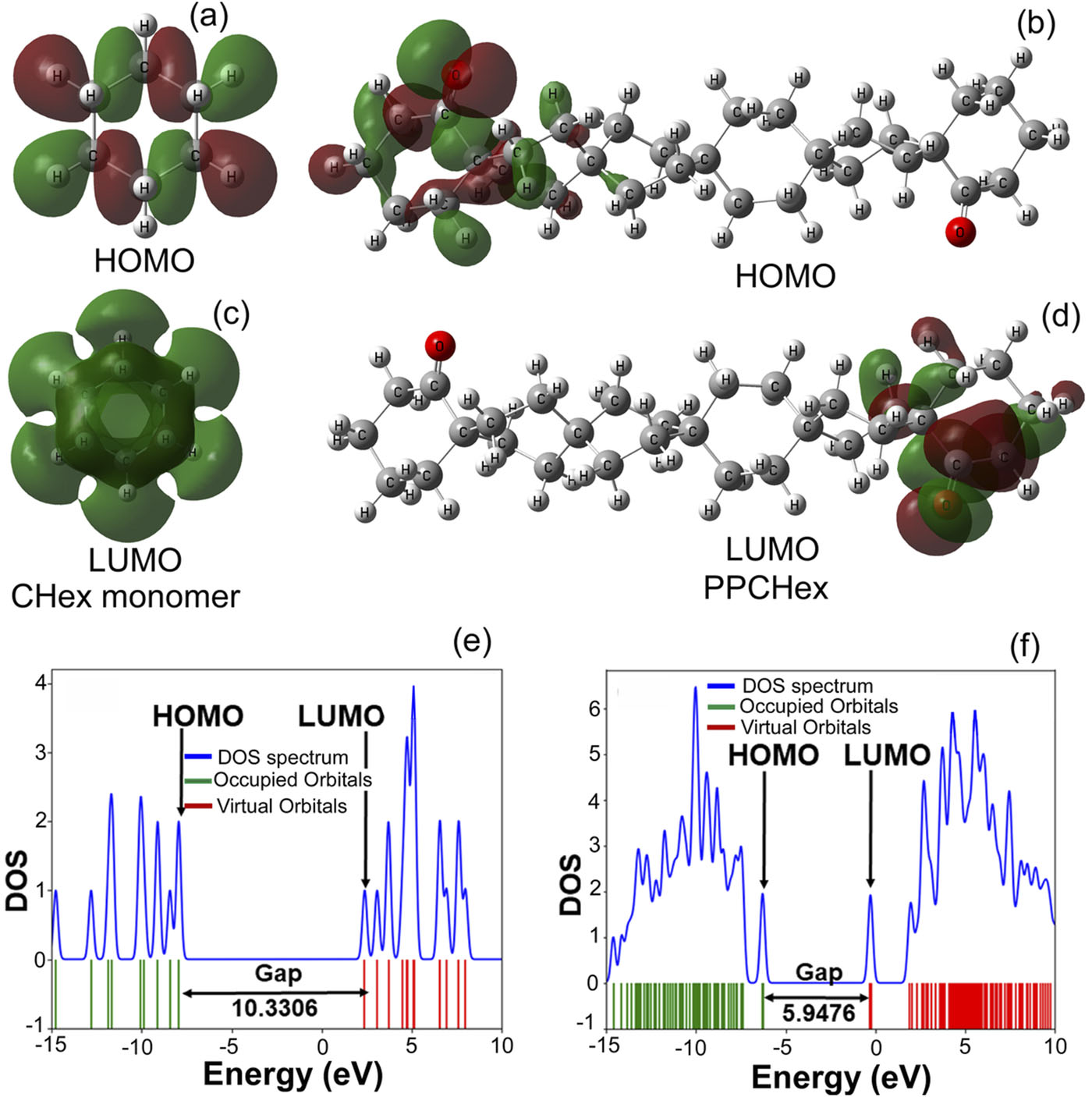
  • Theoretical calculation
  • Material property prediction
  • Process parameter optimization using DOE

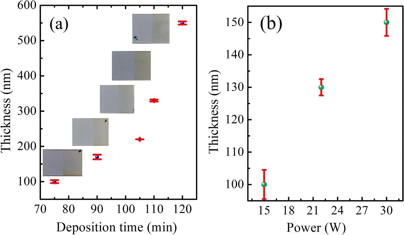
Optimized parameters: Plasma power, Pressure, Deposition condition, Film thickness, Processing window

Established: Material Structure → Plasma Chemistry → Film Property Relationship

3. Thin Film Morphology Characterization

SEM & AFM Metrology

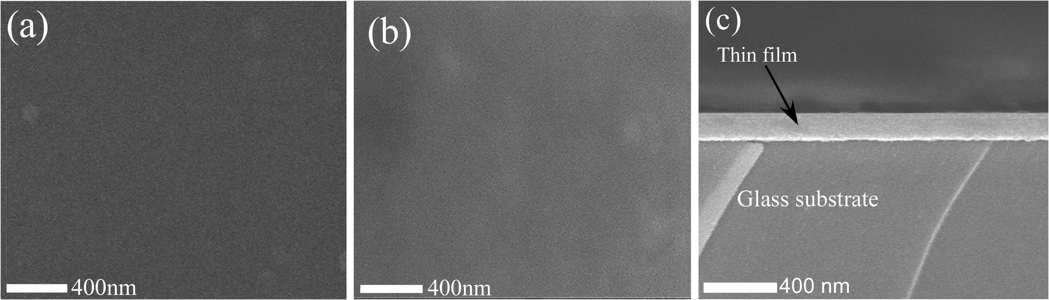
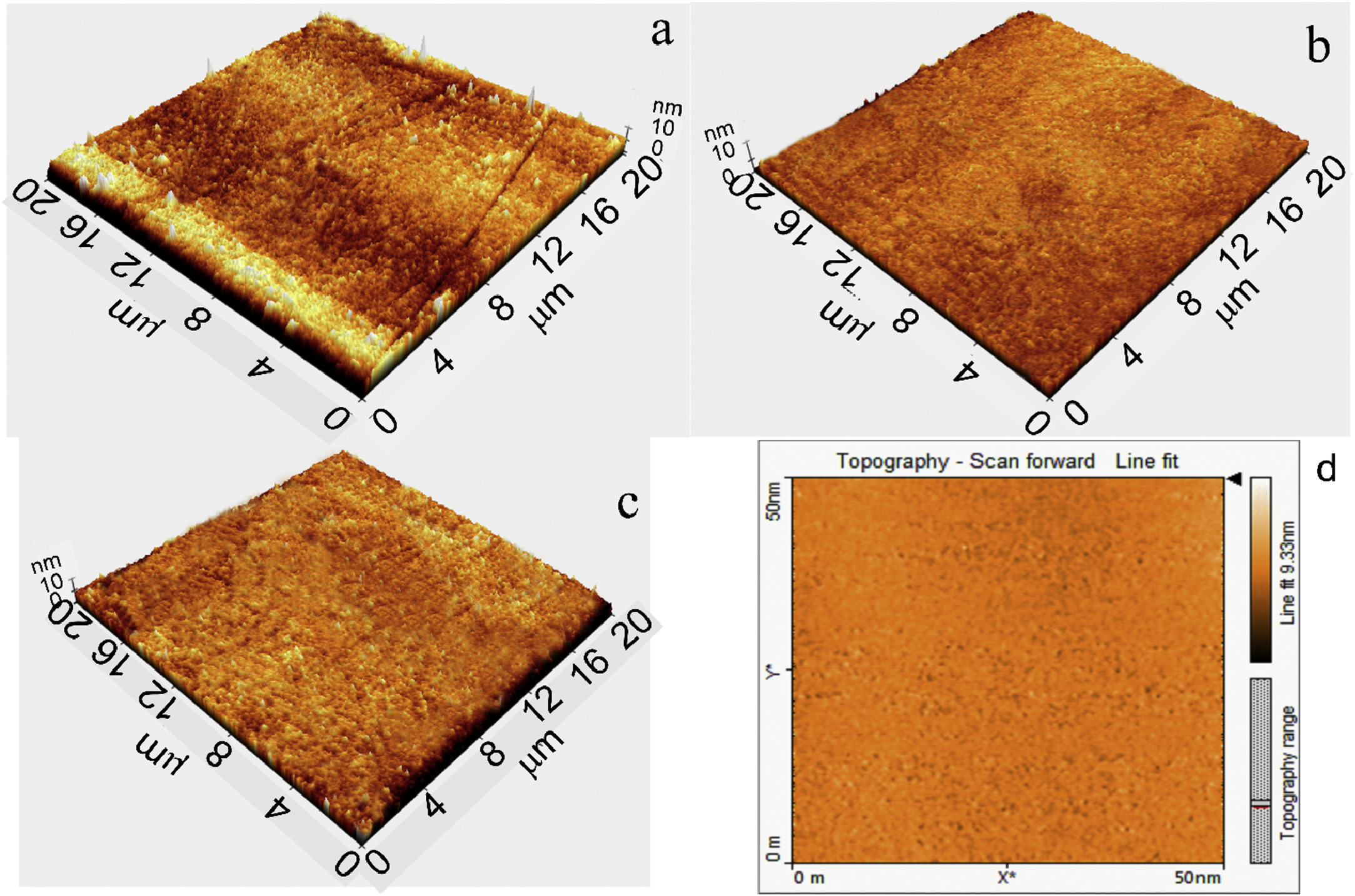
SEM and AFM were used for metrology-driven process optimization.

  • SEM: Surface morphology, Film uniformity, Defect inspection
  • AFM: Surface roughness, Nanostructure analysis, Film quality evaluation

Root cause analysis identified morphology-related process variation and optimized PECVD conditions for improved repeatability.

4. Film Stoichiometry & Chemical Composition Analysis

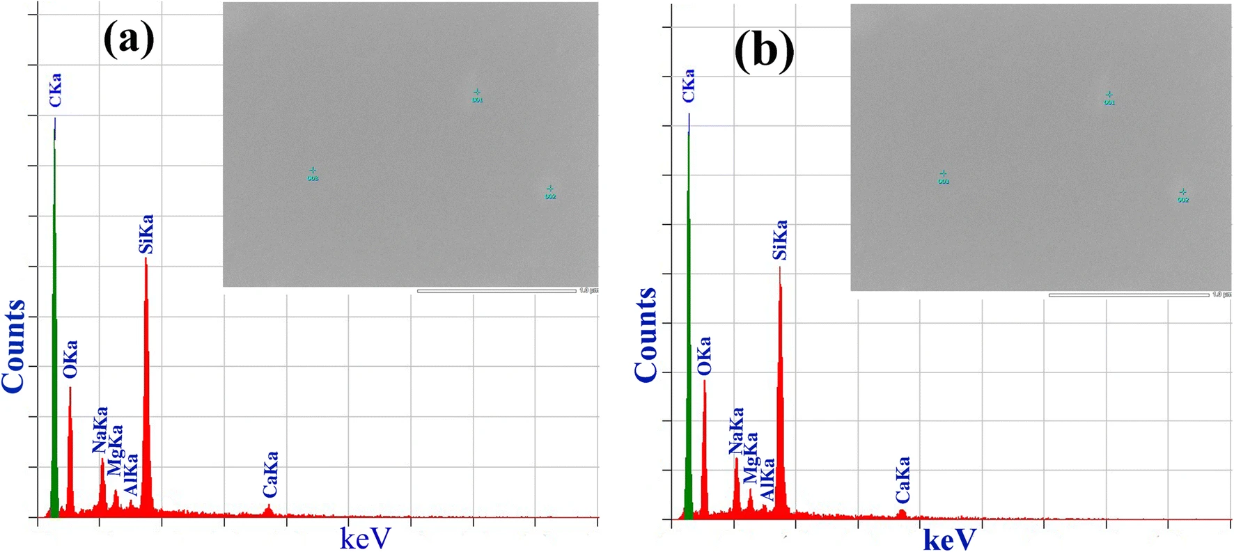
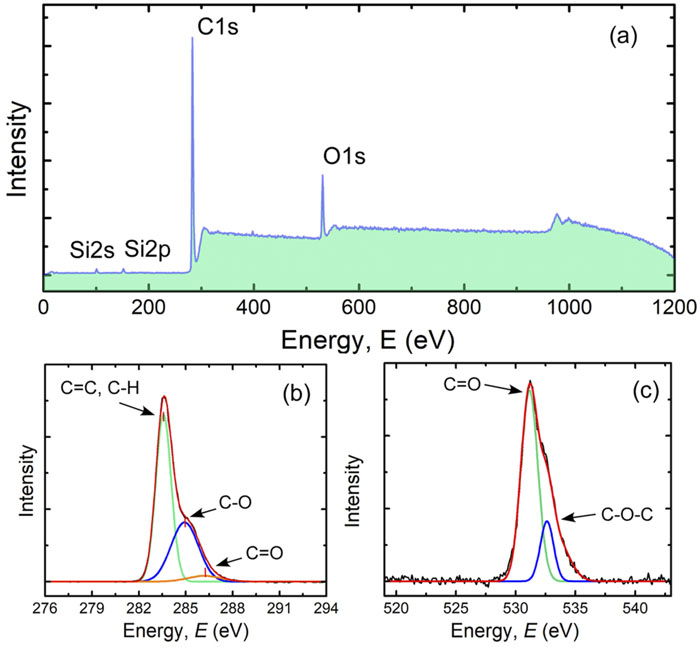
EDS and XPS were performed to analyze: Elemental composition, Chemical bonding states, Surface chemistry, Plasma-induced chemical modification

Used these results to optimize chemical structure and improve film reproducibility.

5. Thermal Stability & Reliability Analysis

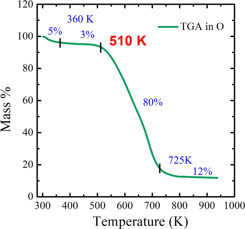
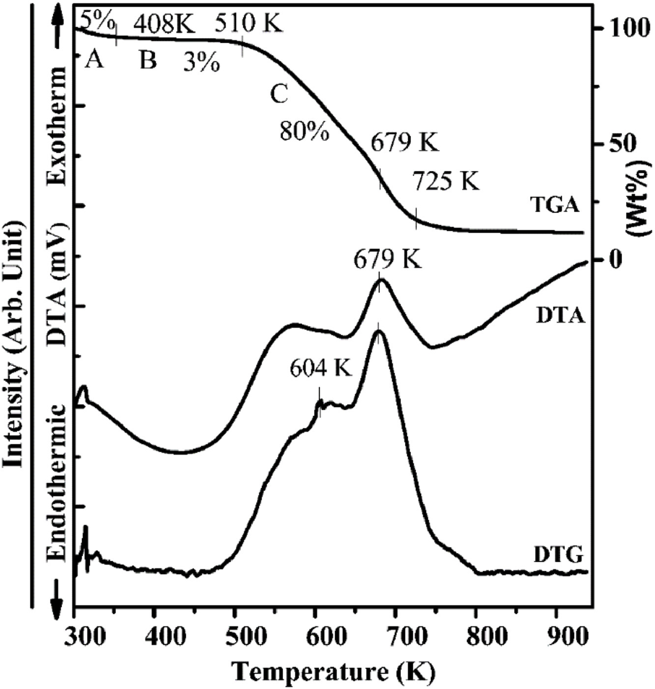
Thermal reliability was investigated using TGA/DTA analysis.

Studied: Decomposition temperature, Thermal degradation pathway, Material stability, Temperature-dependent reliability

Established: Polymer Structure → Thermal Stability → Device Reliability

6. Chemical Structure Analysis

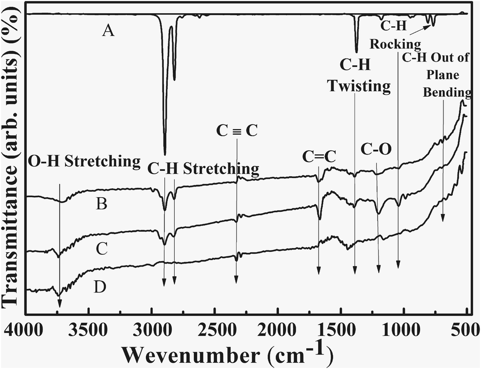
FTIR Vibrational Mode Study

FTIR spectroscopy was used to investigate: Chemical bonding, Molecular vibration modes, Functional groups, Thickness-dependent structural changes

Used FTIR results to optimize plasma polymer network formation.

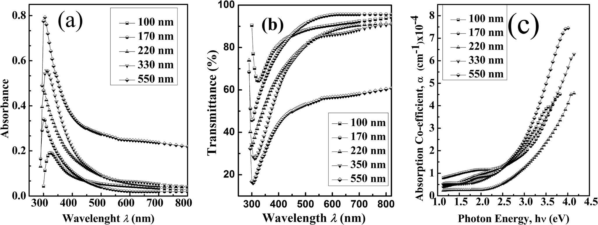
7. Optical Property Characterization

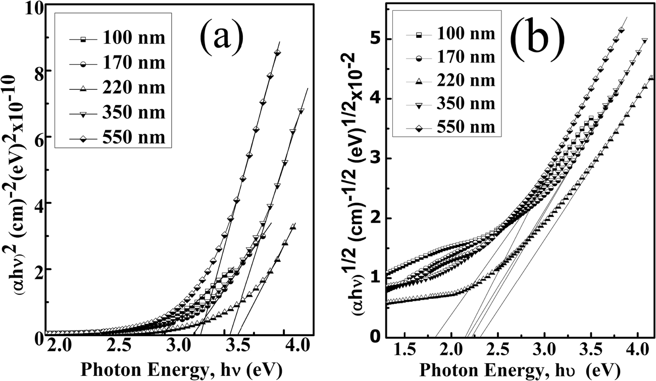
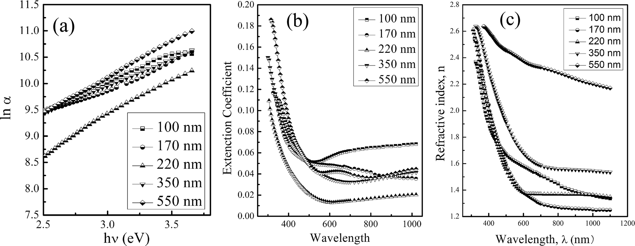
Optical metrology was performed to analyze: Optical absorption, Transparency, Electronic structure, Band gap engineering, Extinction coefficient

Correlation developed: Chemical Structure → Optical Properties → Device Performance

8. DC Electrical Measurement & Conduction Mechanism Analysis

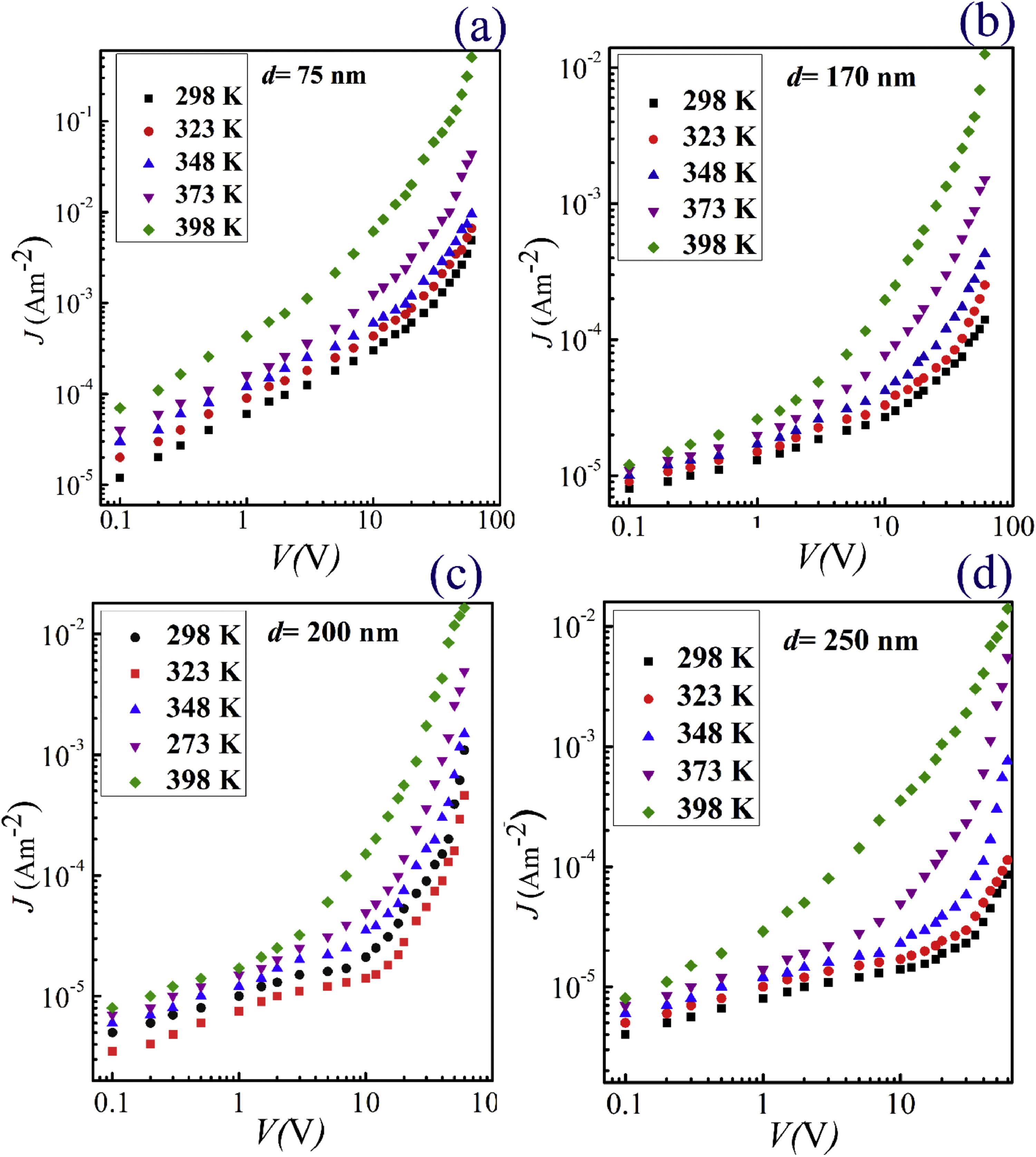
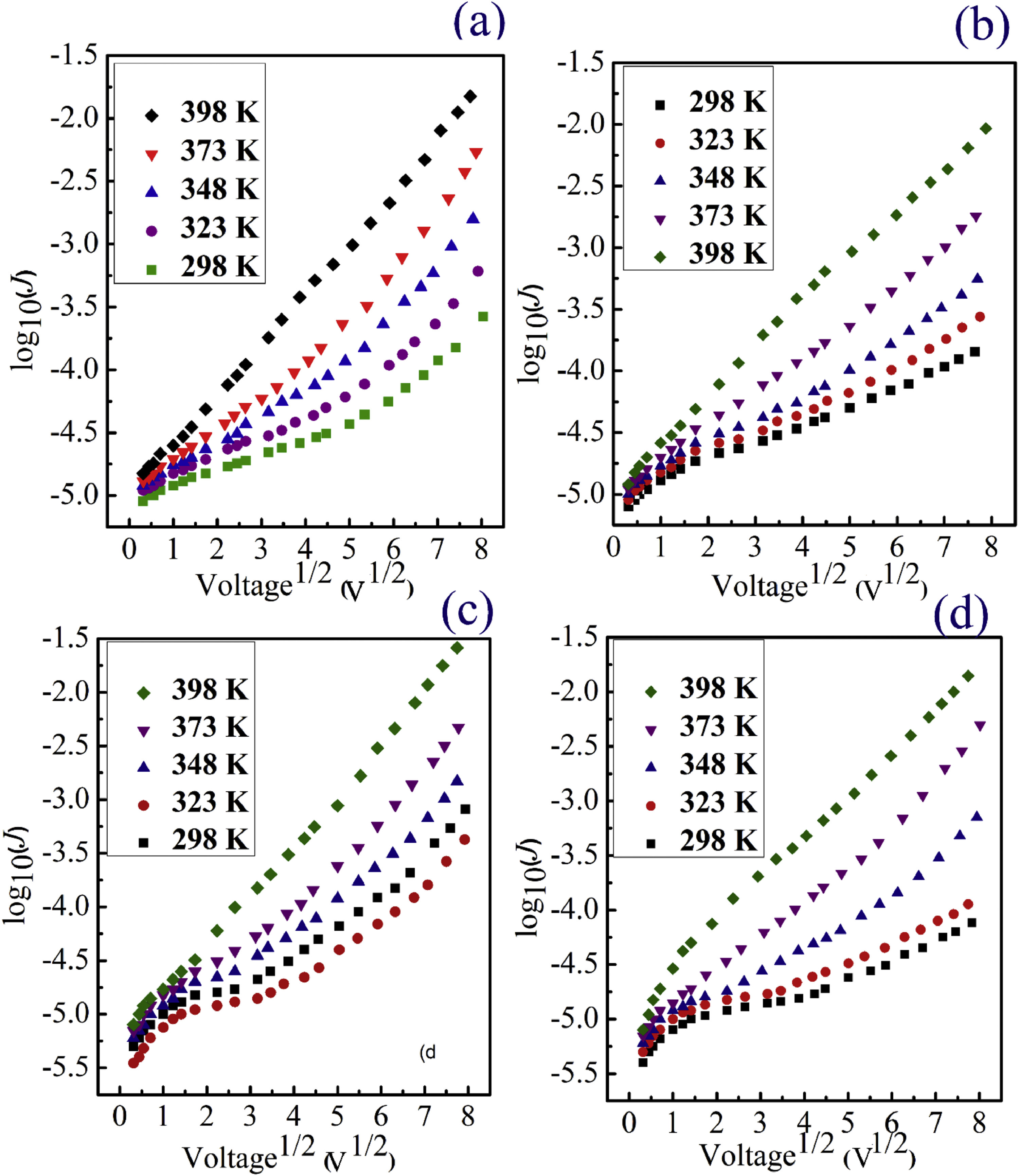
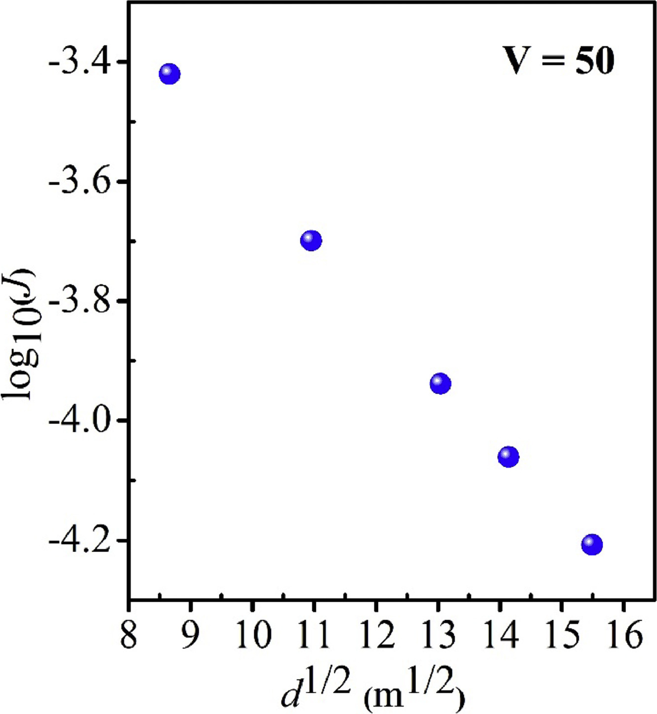
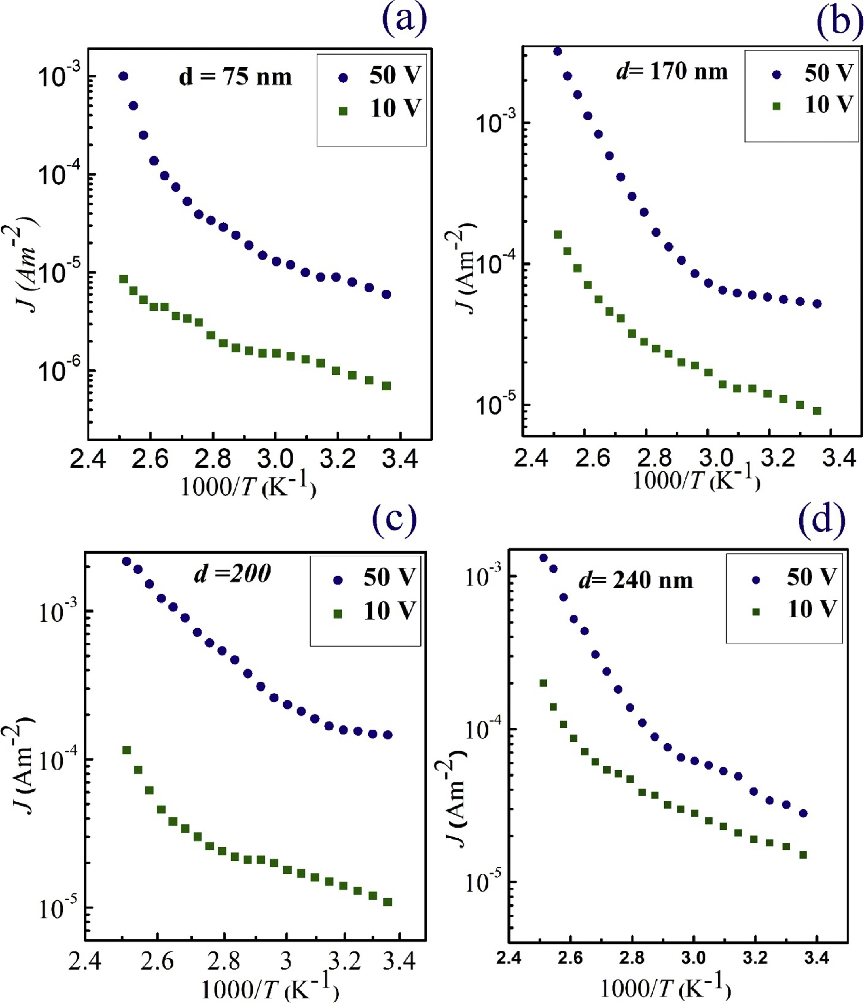
Electrical characterization investigated: Leakage current, Current density, Thickness effect, Charge transport behavior

Conduction mechanisms studied: Ohmic conduction, Space charge limited conduction, Schottky emission, Poole–Frenkel emission

Identified relationship: Film Chemistry → Trap States → Electrical Performance

9. AC Electrical Measurement & Dielectric Properties

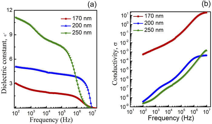
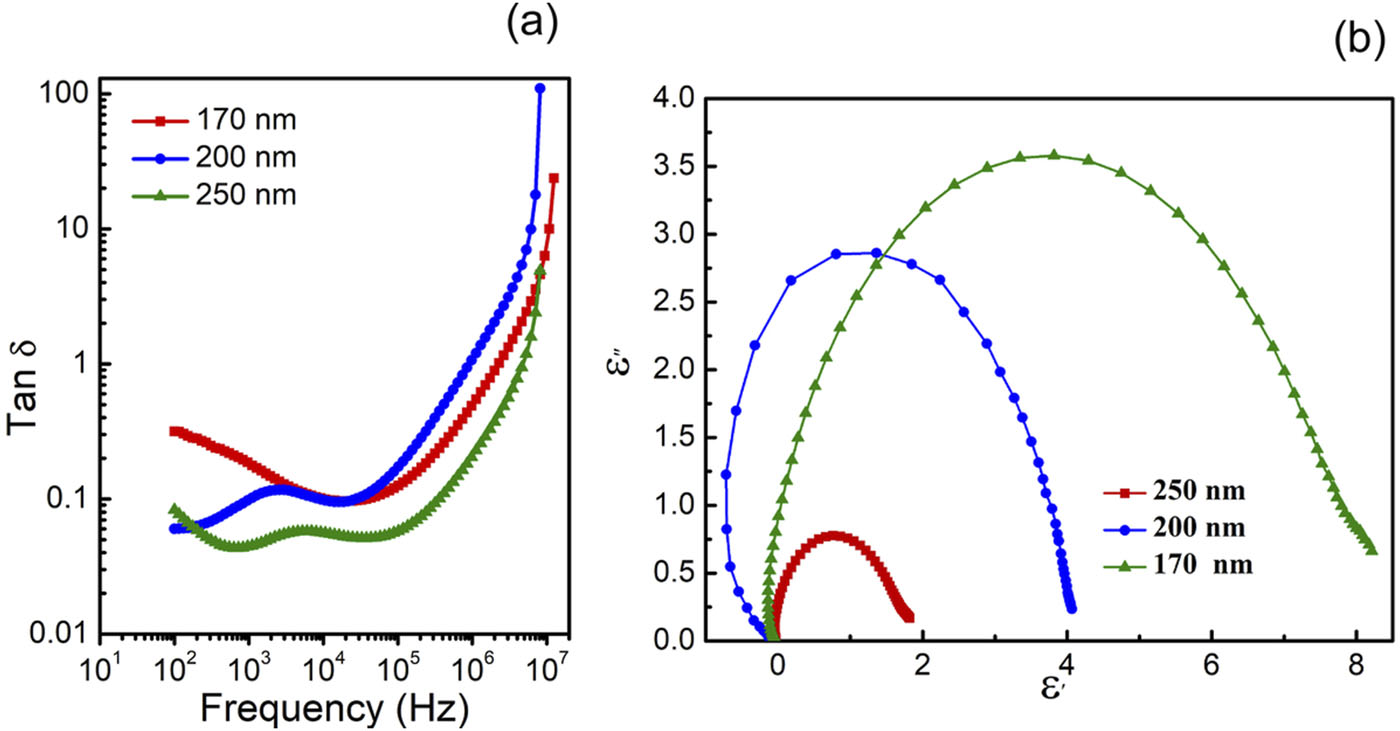
AC electrical characterization evaluated: Dielectric constant, Capacitance response, Frequency-dependent behavior, Dielectric loss, Polarization mechanism

Optimized films showed improved dielectric stability and electrical reliability.

Final Project Outcome

Successfully demonstrated a complete semiconductor thin-film engineering cycle:

Material Selection → Computational Prediction → PECVD Fabrication → DOE Process Optimization → SEM/AFM/XPS/EDS/FTIR/UV–Vis/TGA Electrical Metrology → Root Cause Analysis → Reliable Thin Film Process Development

Metrology & Skills

  • PECVD plasma processing
  • Thin film process development
  • DOE optimization
  • Semiconductor metrology
  • Failure analysis
  • Root cause investigation
  • Electrical characterization
  • Reliability engineering
  • Process–structure–property optimization
  • SEM & AFM
  • EDS & XPS
  • FTIR spectroscopy
  • TGA/DTA thermal analysis
  • UV-Vis optical characterization

Relevant Publications

  1. Microstructural, compositional, topological and optical properties of plasma polymerized cyclohexane amorphous thin films (Springer)
  2. Topological properties and direct current electrical charge transport mechanism of plasma polymerized cyclohexane thin films (ScienceDirect)
  3. Molecular dynamics, transport property, and surface stoichiometry of plasma polymerized cyclohexane thin films (AIP Advances)

Disclaimer: Some figures in this project story are taken from the relevant published journals referenced here, some are taken during the project while it was running (unpublished), and some are currently under review.
MWCNT-Based Smart Shoe Platform: From Material Engineering to Wearable Biomedical Device

Jump to published articles of this project

1. Phase 1: Material Innovation

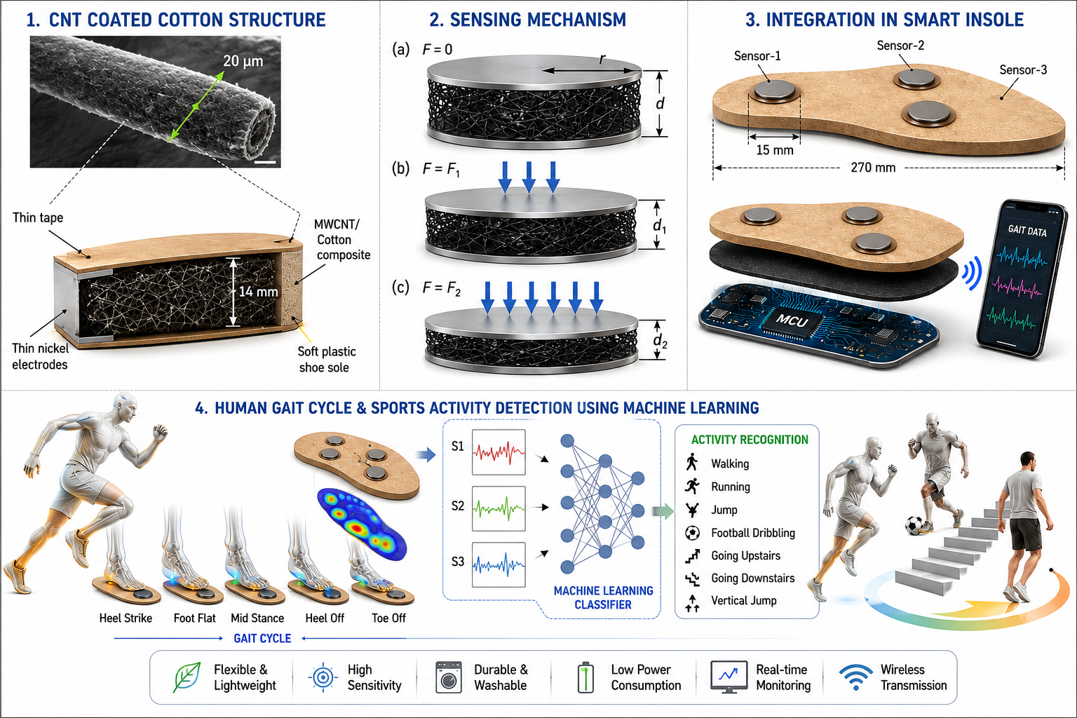
Why I selected wearable sensors: There is a critical need for continuous health monitoring in everyday life. However, conventional rigid sensors are uncomfortable and lack the flexibility required for human motion. My research hypothesis was that flexible, nanomaterial-coated everyday fabrics could serve as high-performance, comfortable wearable sensors.

Selection of MWCNT + cotton fiber: Carbon Nanotubes (CNTs) were selected due to their high conductivity, high aspect ratio, and mechanical robustness.

Problem: CNTs suffer from severe aggregation and poor dispersion.

Solution: I applied citric acid and oxygen plasma functionalization to introduce COOH/OH functional groups. This created a highly stable CNT ink, optimizing the cotton coating mechanism for uniform, durable sensor layers.

2. Material Metrology & Structural Characterization

Material characterization was performed to understand the CNT-fiber interaction and pressure sensing mechanism.

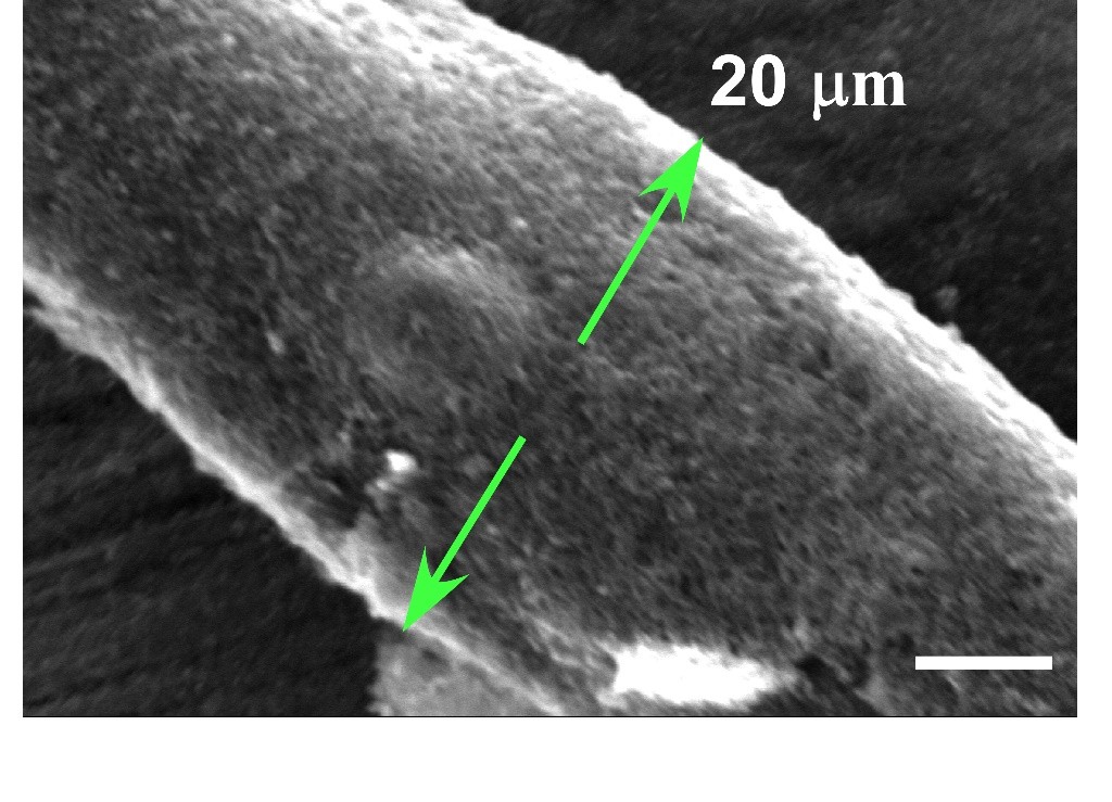
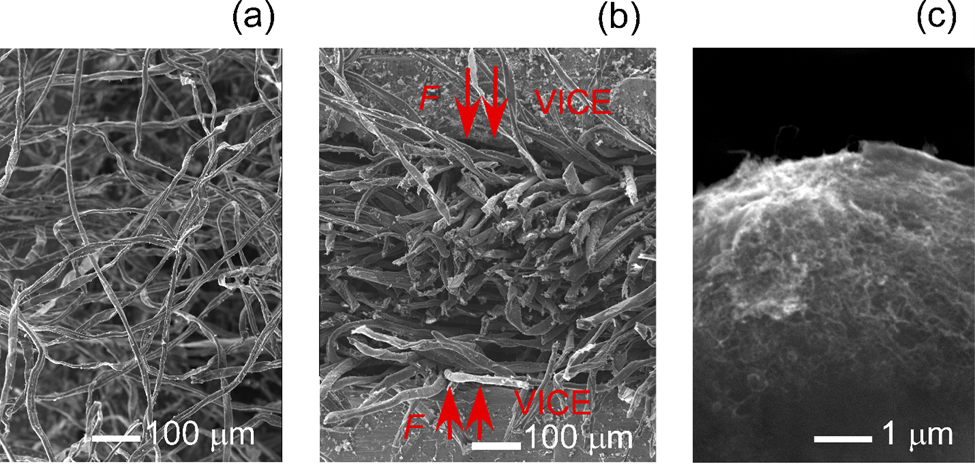
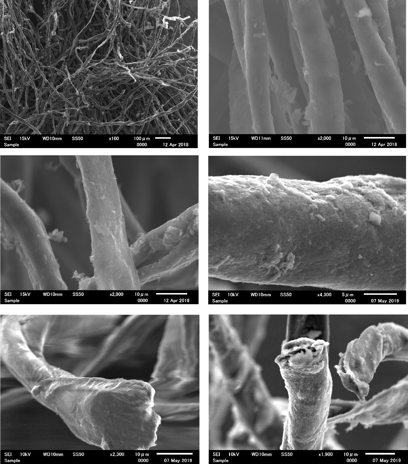
SEM Analysis: Used for cotton fiber morphology, CNT coating uniformity, surface coverage analysis, and fiber network structure after compression.

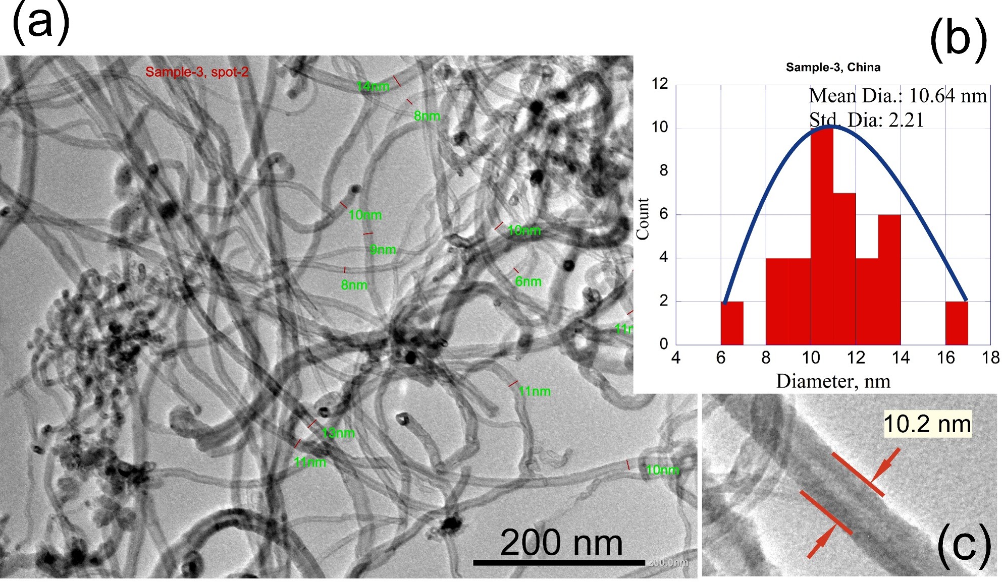
TEM Analysis: Used for CNT morphology confirmation, nanotube network formation, and conductive pathway analysis.

SEM/TEM results confirmed successful CNT attachment on cotton fibers, forming a conductive nanoscale network.

3. Root Cause Analysis: Pressure Sensing Mechanism

Initial Challenge: Sensor performance depended strongly on mechanical compression behavior and CNT network formation.

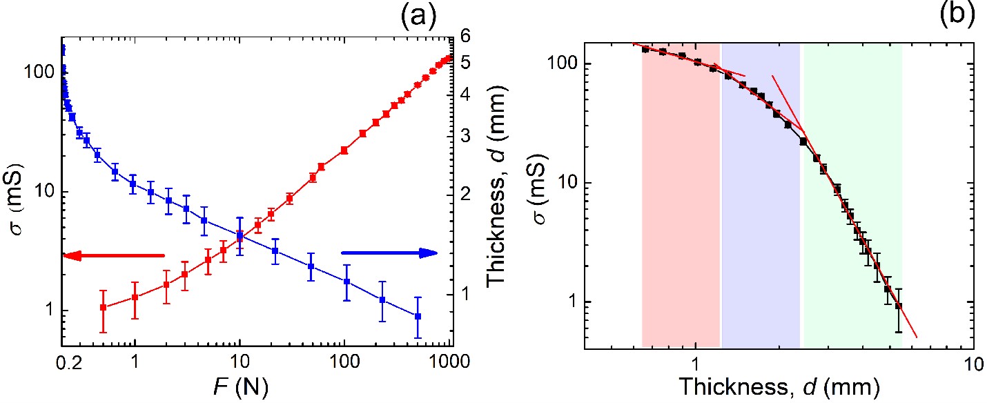
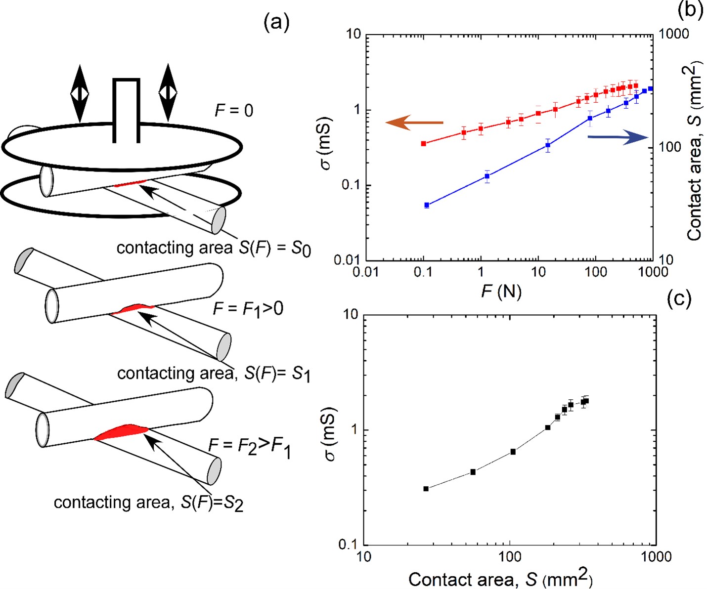
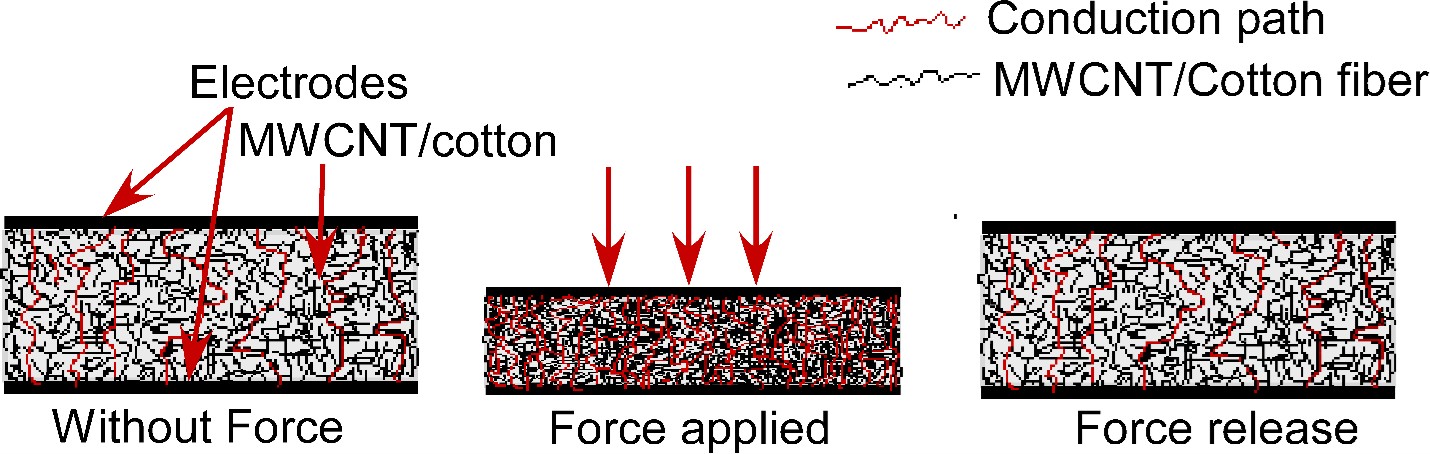
Root cause investigation: Using SEM/TEM and electrical-force characterization, I identified that sensor response originated from:

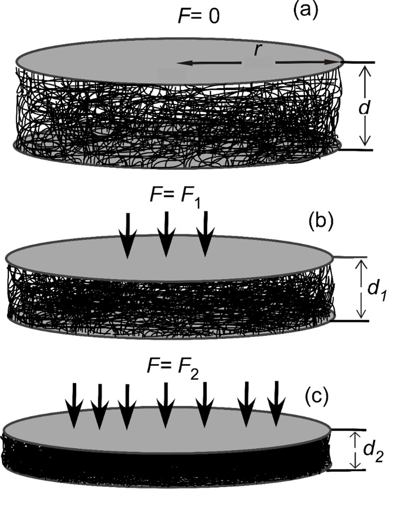
  • Increased CNT-to-CNT contact points during compression
  • Reduced tunneling distance between CNT networks
  • Increased conductive pathways
  • Larger fiber contact area under applied pressure

Pressure applied ➔ Fiber compression ➔ CNT network connection increases ➔ Resistance decreases ➔ Electrical signal generated

This mechanism study enabled optimization of sensitivity and repeatability.

4. Sensor Performance Optimization

Electrical and mechanical validation included: Pressure sensitivity measurement, Loading/unloading response, Response and recovery time, Hysteresis analysis, Repeatability testing, and Long-term durability (>11,000 cycles).

Optimization improved:

  • Sensitivity
  • Response stability
  • Mechanical reliability
  • Wearable compatibility

5. Smart Shoe Integration & Human Activity Testing

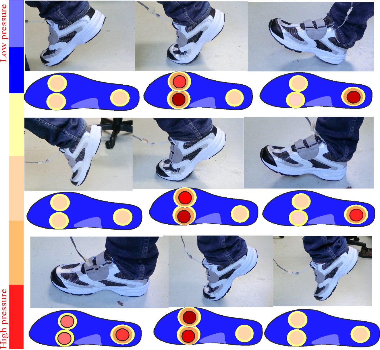
After sensor optimization, multiple sensors were integrated into a shoe platform for real-time biomechanical monitoring.

Sensor locations were selected to capture: Heel pressure, Toe pressure, Forefoot loading, Pressure shifting, Center of gravity movement.

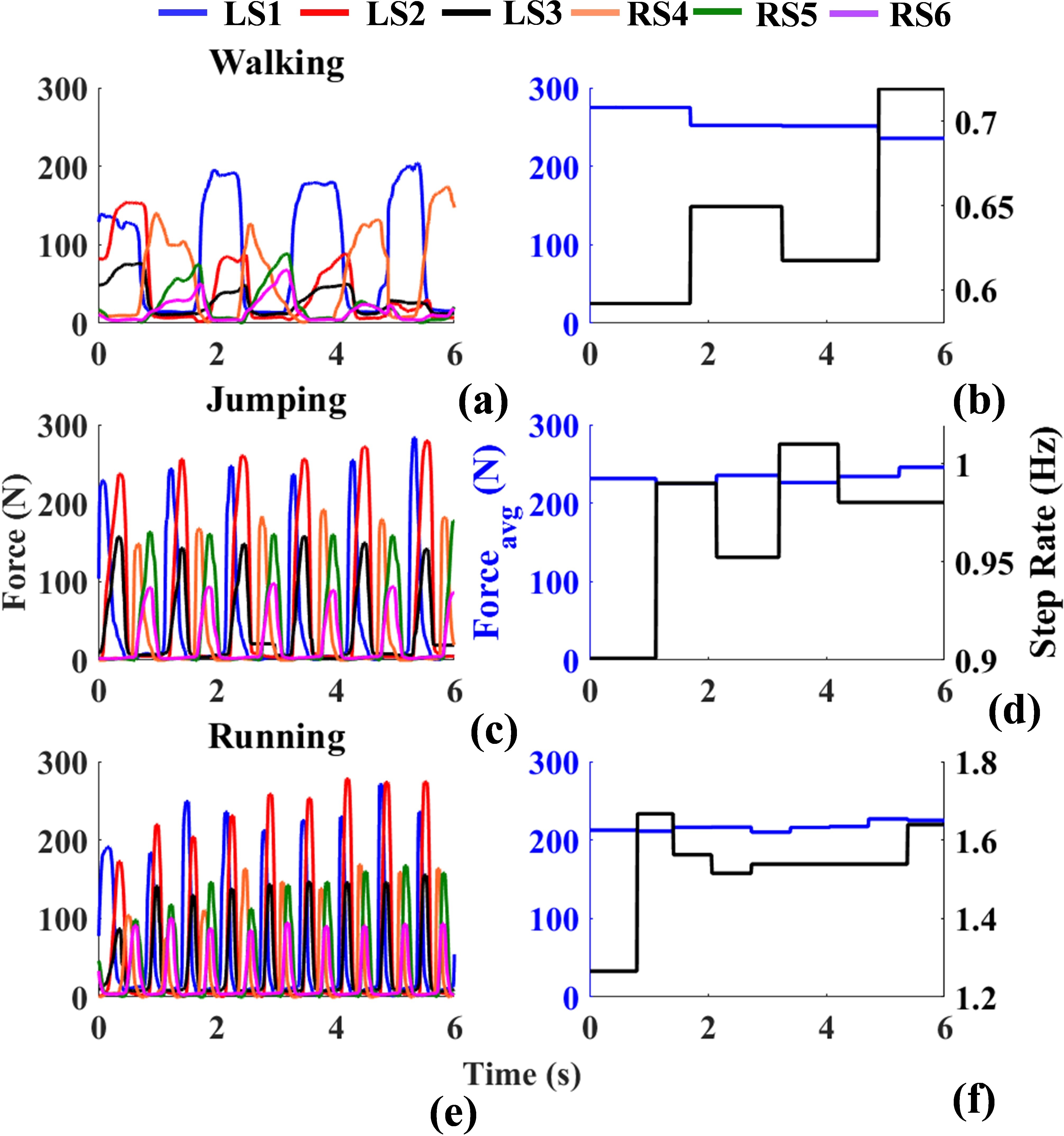
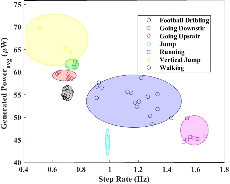
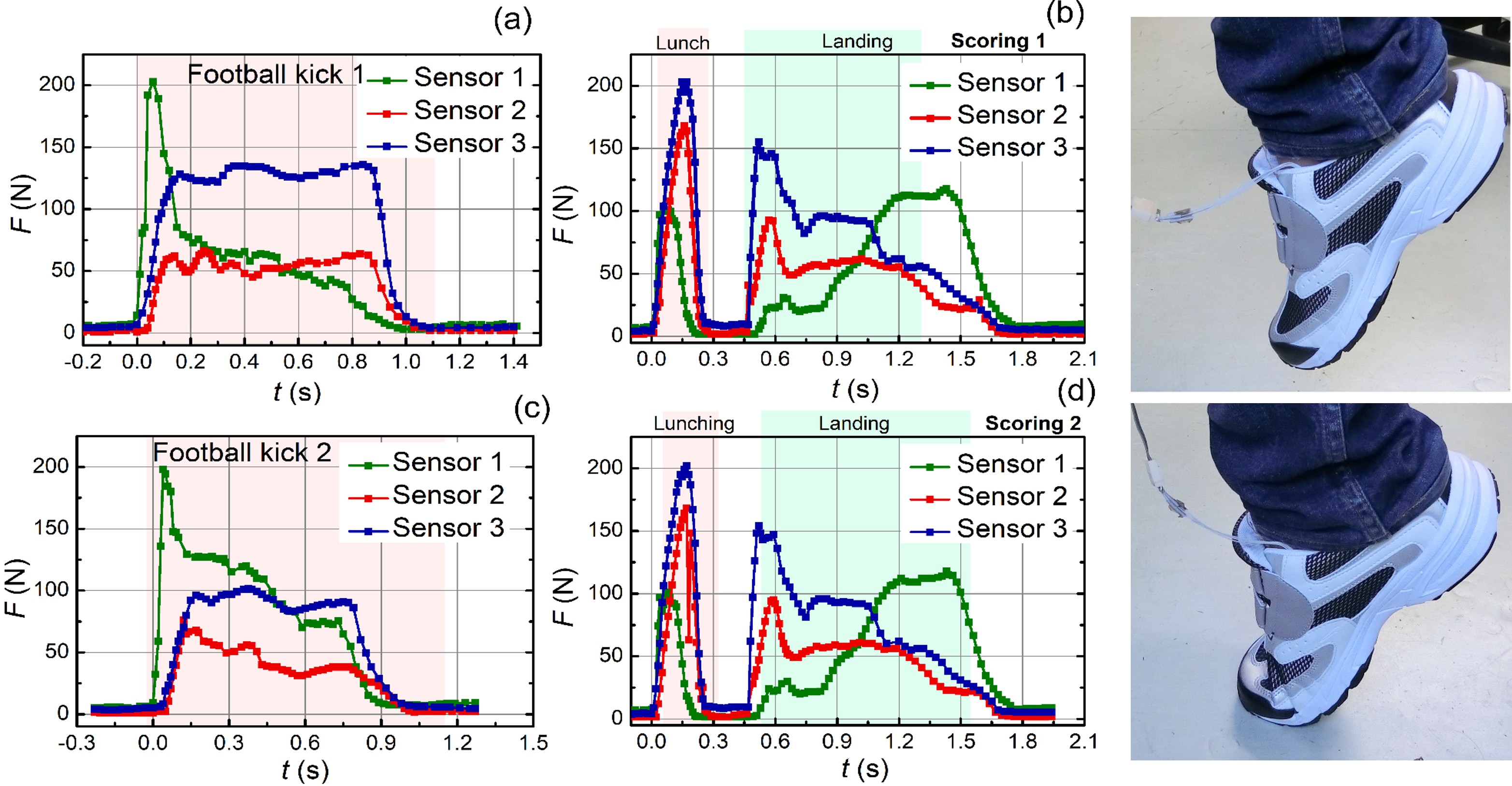
Human Motion Validation: The smart shoe platform was tested during Standing, Walking, Running, Jumping, and Different activity patterns.

The system successfully monitored: Step cycle, Ground contact force variation, Loading/unloading behavior, Gait characteristics, Body movement patterns.

6. Advanced System Development

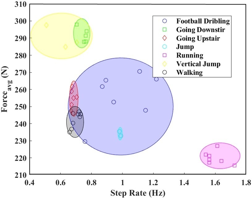
The platform was further expanded toward: Self-powered wearable sensors, Energy harvesting from body motion, Breathing monitoring, Muscle activity sensing, Human activity classification.

Machine learning analysis: Feature extraction, MRMR feature selection, Activity classification.

Project Outcome:

  • Developed complete wearable pressure sensor platform
  • Established CNT composite material optimization process
  • Performed DOE-based sensor improvement
  • Used SEM/TEM-driven root cause analysis
  • Integrated sensor into functional smart shoe system
  • Demonstrated real-world human activity monitoring

Videos

Watch the carbon nanotube functionalization process and the smart shoe in action.

Publications

Detailed findings from this project have been published in the following peer-reviewed journals:

Metrology & Skills

  • pressure sensing characterization
  • electrical measurements
  • device response analysis
  • sensor fabrication
  • MWCNT-coated cotton fiber sensor development
  • load / pressure calibration
  • human activity monitoring
  • data analysis
  • wearable sensor validation
  • performance and repeatability testing
  • force / load calibration
  • electrical characterization
  • sensitivity analysis
  • response stability testing
  • device fabrication
  • performance validation
  • health-monitoring application testing
  • XPS
  • SEM
  • AFM
  • EDX
  • FTIR
  • UV-Vis
  • multiple-beam interferometry
  • DC electrical measurements
  • impedance analysis
  • capacitance
  • conductance
  • dielectric characterization
  • DTA
  • TGA
  • DTG
  • film stoichiometry analysis
  • surface chemistry analysis

Relevant Publications & Output

Detailed findings from this project have been published in the following peer-reviewed journals:

  1. Journal of Sensors (2019)
  2. Surface and Coatings Technology (2020)
  3. Analysis & Sensing (2024)

Disclaimer: Some figures in this project story are taken from the relevant published journals referenced here, some are taken during the project while it was running (unpublished), and some are currently under review.
Wearable Smart Ring for Continuous Blood Pressure Monitoring

Jump to published articles of this project

Why Do We Need a Wearable Blood Pressure Monitoring Ring?

Ask yourself one question: When was the last time you measured your blood pressure?

For most people, the answer is only during a doctor visit or occasional home measurement. However, between those measurements, we do not continuously know our cardiovascular condition.

Conventional cuff-based BP monitors are accurate, but they are bulky, uncomfortable, and not accessible anytime and anywhere. This limitation creates the need for a wearable solution that can continuously support cardiovascular health monitoring.

Technology Gap in Current Smart Rings

Commercial smart rings such as Oura Ring and other wearable rings have created a new generation of health monitoring by tracking heart rate, sleep, activity, and physiological trends.

However, existing smart rings still cannot directly measure absolute systolic and diastolic blood pressure because true BP measurement requires applying controlled pressure to interact with and partially occlude the artery.

Without controlled mechanical squeezing of the artery, direct cuff-like BP measurement is extremely challenging.

Our Innovation: Actuated Smart Ring for Direct Blood Pressure Measurement

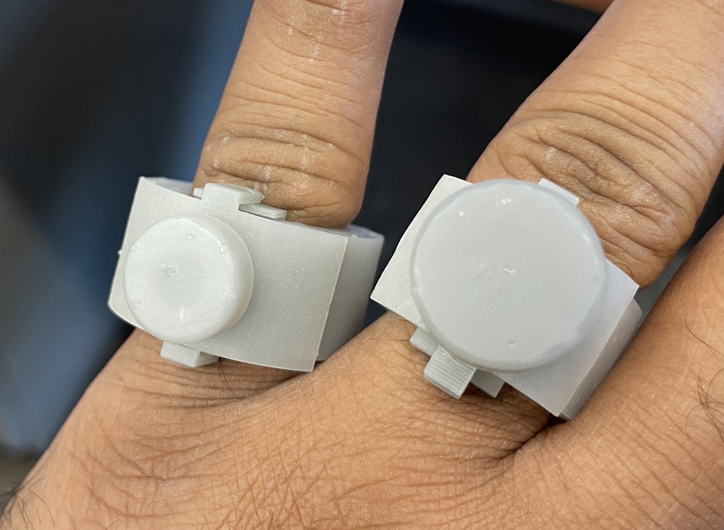
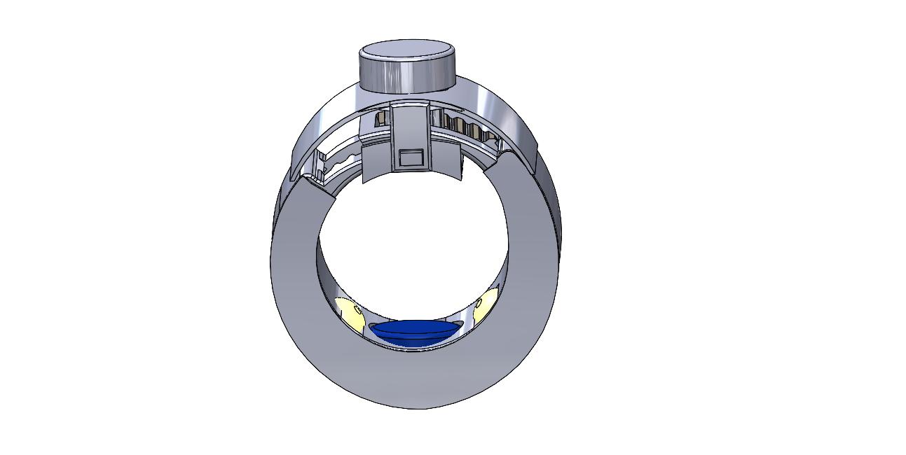
We developed a smart ring with a custom-designed mechanical actuator capable of applying controlled radial pressure on the finger to occlude the digital artery.

This approach miniaturizes the fundamental principle of conventional cuff-based BP measurement into a wearable ring platform.

Key developments:

  • Custom mechanical actuator design
  • Controlled finger artery compression mechanism
  • Pressure and optical sensing integration
  • Signal processing for systolic and diastolic BP estimation

This actuator concept can potentially be integrated into future commercial smart ring platforms to enable direct BP monitoring.

Mechanical Design Optimization & Engineering Development

Several mechanical actuation approaches were designed and evaluated to achieve a compact wearable system.

More than five actuation concepts were investigated with a focus on:

  • Miniaturization
  • Wearability and comfort
  • Repeatable pressure control
  • Reliable artery interaction
  • Compatibility with commercial smart ring architecture

CAD Design and 3D Printing

The mechanical components of the smart ring were designed using CAD software and fabricated via high-resolution 3D printing. The systematic development and optimization process included:

  • CAD design of individual ring components separately
  • Design optimization for assembly and functionality
  • Optimization of 3D printing layer thickness for high precision
  • Optimization of UV curing processes to ensure structural integrity
  • Achieving mechanically stable and reusable parts
  • Final assembly of the fully optimized ring for continuous wear and use

Human Subject Validation

The prototype was evaluated through human studies.

Data were collected from more than 25 subjects, and ring-estimated systolic pressure (SP) and diastolic pressure (DP) were compared with conventional cuff BP measurements.

The results demonstrated the feasibility of wearable ring-based BP monitoring with user maneuvers, reducing dependency on occasional cuff measurements.

Impact for Next-Generation Wearable Health Technology

This work provides a pathway from traditional intermittent BP measurement toward convenient wearable cardiovascular monitoring.

The project combines:

  • Wearable medical device design
  • Mechanical actuator engineering
  • Sensor integration
  • Human physiological measurement
  • Data analysis and validation

The technology has potential applications for next-generation smart rings and continuous cardiovascular health platforms.

Metrology & Skills

  • force sensor integration
  • PPG sensor integration
  • IMU integration
  • MATLAB data analysis
  • custom DAQ / data acquisition
  • BP estimation algorithm development
  • device validation
  • human subject data collection under IRB
  • absolute blood pressure measurement studies
  • 3D ring design
  • 3D printing
  • mechanical actuator design
  • circuit integration
  • signal processing
  • real-time measurement workflow development

Relevant Publications & Output

  1. Md Abdul Momin et al., Wireless Finger-Worn Ring for On-Demand Measurement of Absolute Blood Pressure. Postdoctoral Research Symposium, University of Pittsburgh (2024)
  2. Md Abdul Momin, Shipeng Wang, Mahdi Jazini, Mark Freithaler, Shahin Hashemkhani, Graham Ethan Hoover, Yuyang Li, In Hee Lee, Feng Xiong, Ramakrishna Mukkamala*, A Finger Worn Ring for On-Demand Measurement of Absolute Blood Pressure, Submitted to IEEE Transactions on Biomedical Engineering (April 2026).

Disclaimer: Some figures in this project story are taken from the relevant published journals referenced here, some are taken during the project while it was running (unpublished), and some are currently under review.
Experimental and First Princple Computation of Thin Films

Jump to published articles of this project

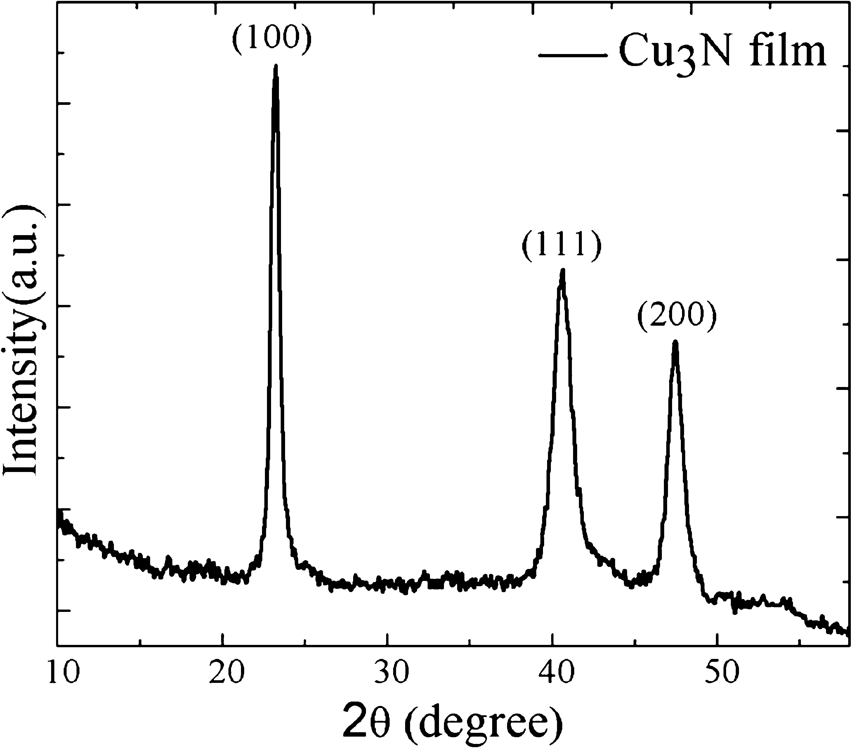
In this project, I investigated the structural, electronic, and optical properties of copper-based thin films (Cu3N and Cu-TiC) through a combination of computational modeling and experimental validation.

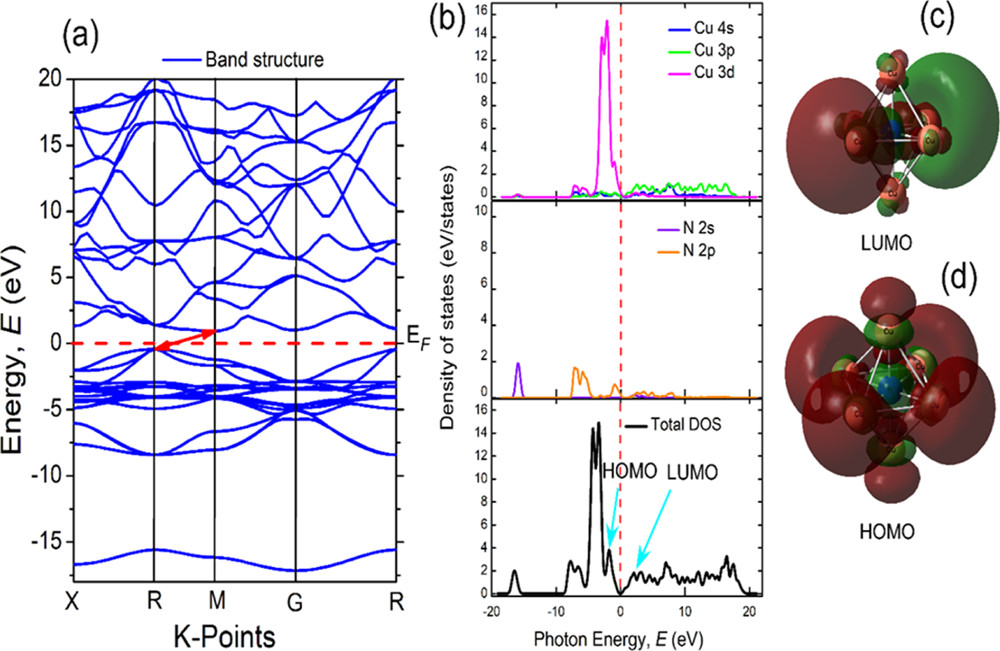
Using the Density Functional Theory (DFT) framework with the Local Density Approximation (LDA) and the Hubbard (U) term, I modeled the crystal structures, band structures, and electron density distributions of these materials. The simulations revealed strong hybridization of atomic orbitals in the valence band regions, which significantly influenced the optical and electronic characteristics.

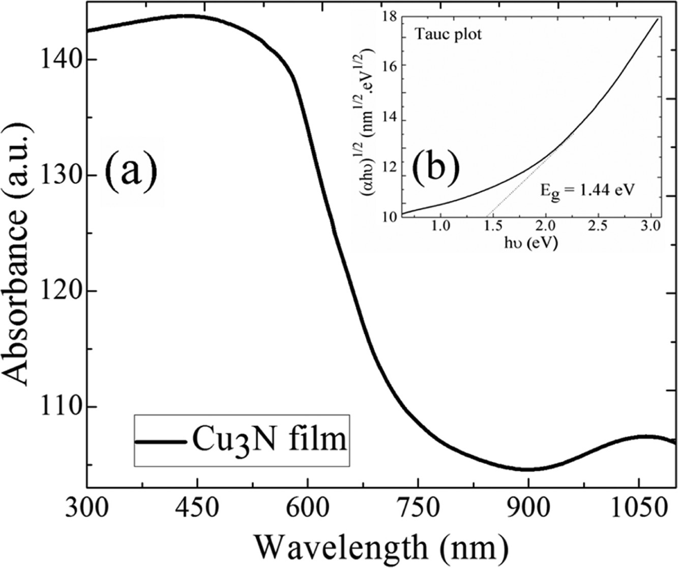
To validate these theoretical models, thin films were deposited on Si substrates using the DC magnetron sputtering technique. Experimental optical characterizations were then performed to extract the optical bandgap and refractive index, which were subsequently compared against the theoretical approximations.

Cu3N Thin Films

Optical and Electronic Structural Properties of Cu3N Thin Films: A First-Principles Study (LDA + U)

A comprehensive first-principles study was conducted on Cu3N thin films using Density Functional Theory (DFT) with the Local Density Approximation and Hubbard (U) term (LDA + U). Band structure analysis revealed strong hybridization of Cu 3d and N 2p orbitals due to their antibonding states in the near-valence band region. Experimentally, DC magnetron-sputtered Cu3N films exhibited a polycrystalline structure with a nonstoichiometric phase. The experimentally determined optical band gap (1.44 eV) and refractive index (2.14) showed excellent agreement with our theoretical approximations.

Cu-TiC Thin Films

Structural and Optical Properties of Cu-TiC Thin Films: a DFT Study

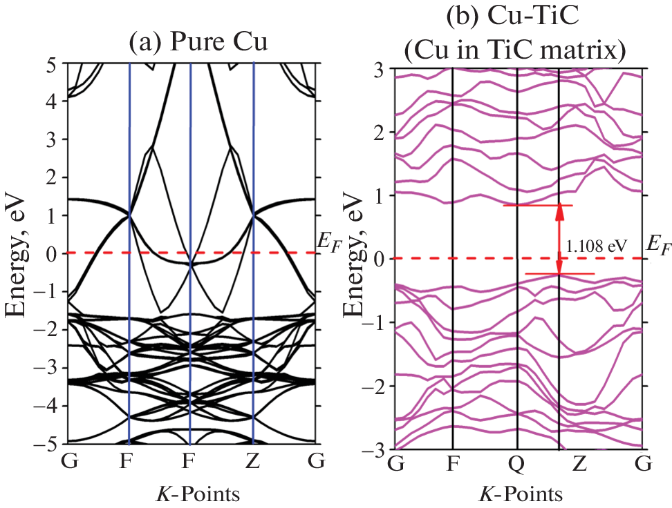
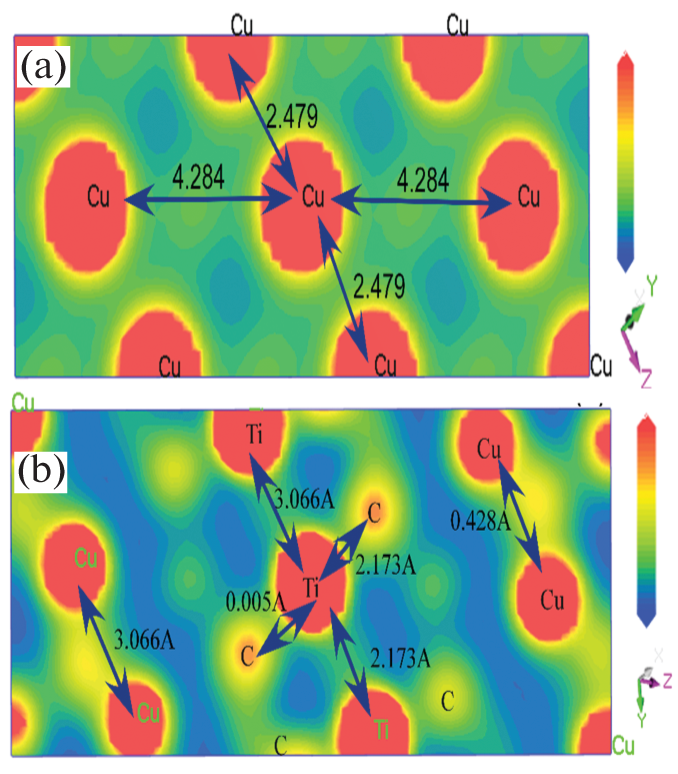
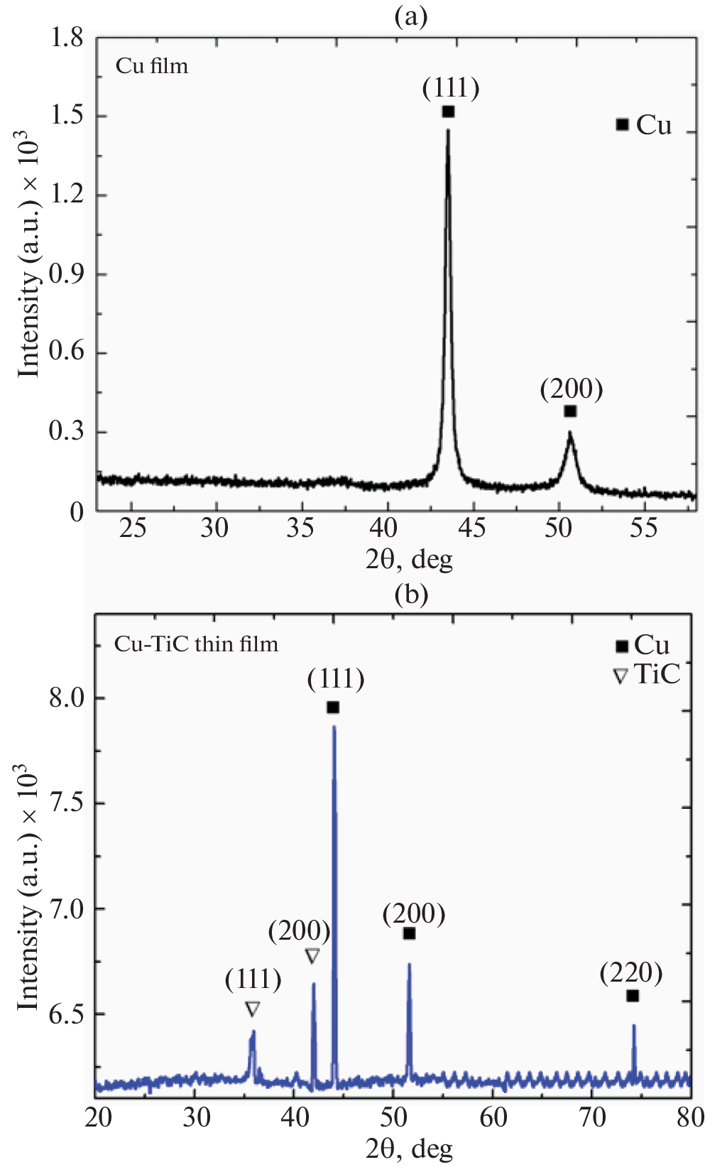
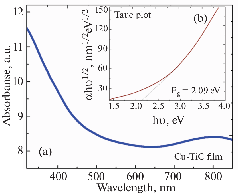
We investigated the structural geometry and electronic properties of Cu-TiC thin films using the DFT framework with LDA. The simulated Cu-TiC band structure demonstrated strong hybridization across Cu-Ti, Cu-Cu, and Cu-C valence band regions. To validate these findings, thin films were deposited on Si via co-sputtering of Cu, Ti, and C targets using DC magnetron sputtering. While the experimentally derived lattice constant aligned closely with the theoretical model, the measured optical bandgap (2.09 eV) highlighted variations from the simulated value (1.10 eV) obtained via linear optical response theory.

CuO and Zn-Doped CuO Thin Films

Structural, optical and electronic properties of CuO and Zn doped CuO: DFT based First-principles calculations

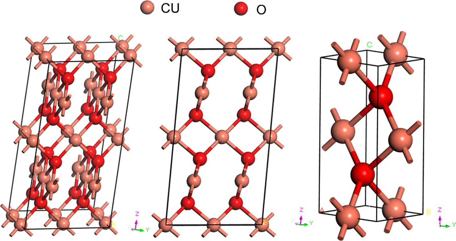
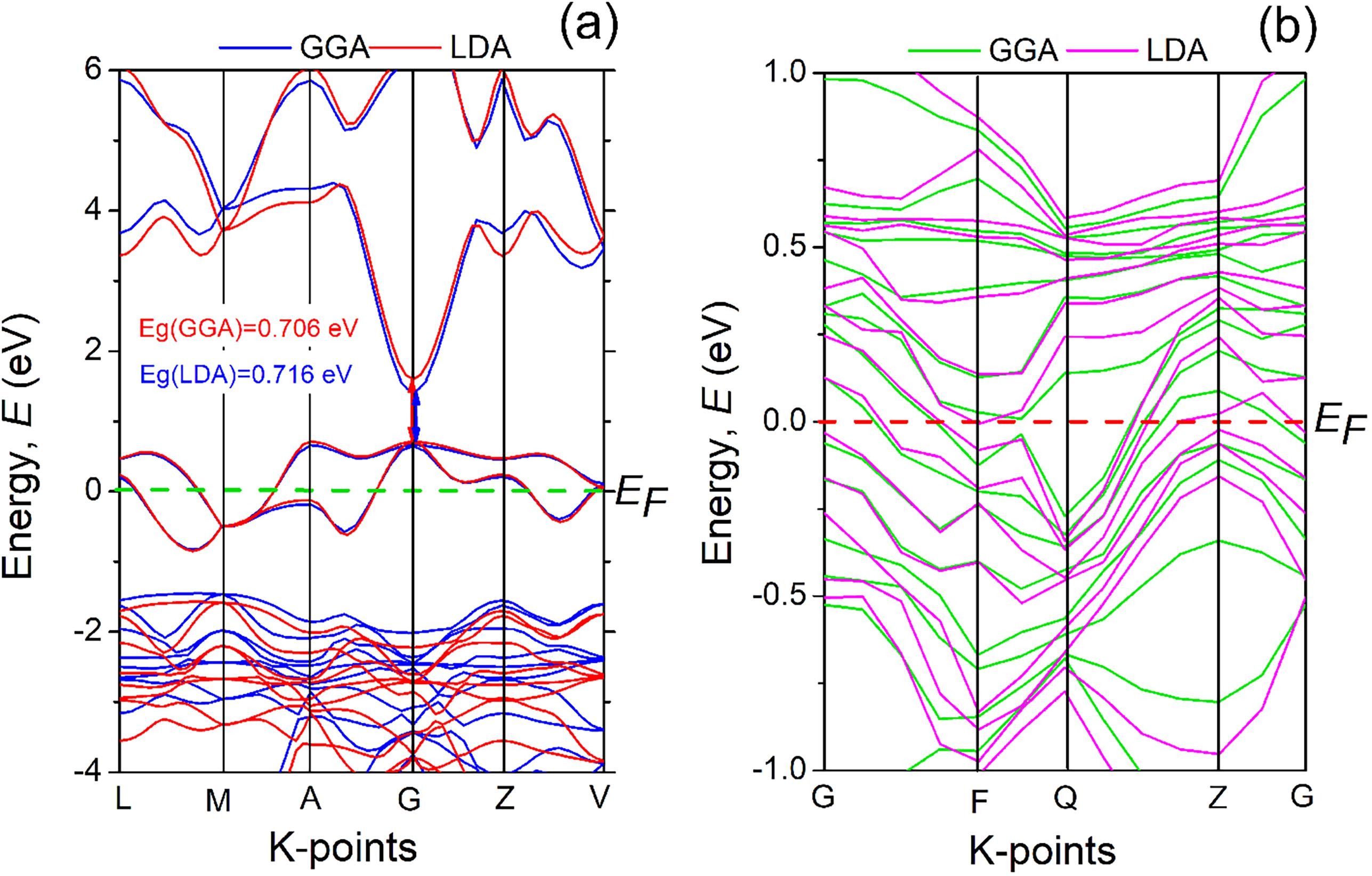
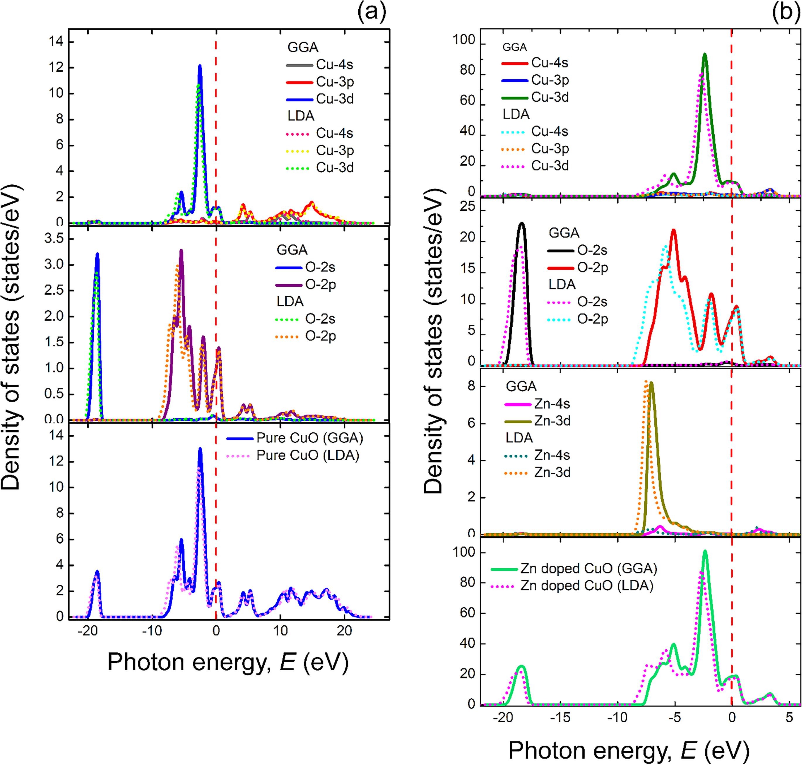
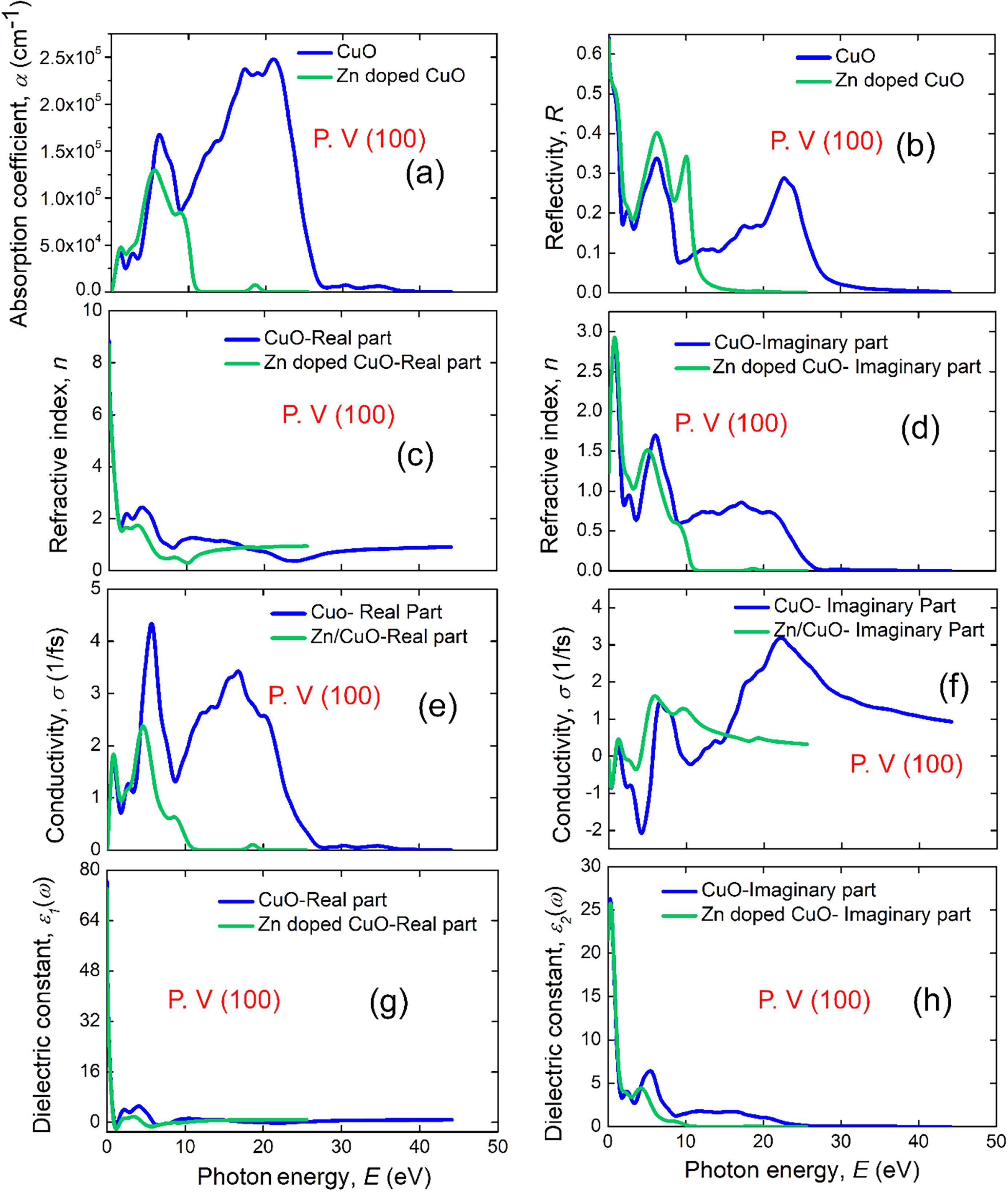
We performed First-principles Density Functional Theory (DFT) calculations using the Cambridge Serial Total Energy Package (CASTEP) to investigate the structural, electronic, and optical properties of CuO and Zn-doped CuO thin films. The computed electronic band structures, alongside Total and Partial Density of States (TDOS/PDOS), revealed a significant transition in the band gap upon Zn doping. Optical simulations demonstrated that both materials are transparent with a small energy gap and exhibit maximum reflectivity in the infrared region. The calculated lattice parameters and band gap values were in good agreement with our experimental data.

Relevant Publications & Output

  1. Optical and Electronic Structural Properties of Cu3N Thin Films: A First-Principles Study (LDA + U) (ACS Omega)
  2. Structural and Optical Properties of Cu-TiC Thin Films: a DFT Study (Semiconductors)
  3. Structural, optical and electronic properties of CuO and Zn doped CuO: DFT based First-principles calculations (Chemical Physics)

Disclaimer: Some figures in this project story are taken from the relevant published journals referenced here, some are taken during the project while it was running (unpublished), and some are currently under review.
Metrology & Skills

  • Density Functional Theory (DFT)
  • First-Principles Calculations (LDA + U)
  • DC Magnetron Sputtering
  • Band Structure & DOS Analysis
  • Optical Characterization
  • UV-Vis Spectroscopy
  • X-Ray Diffraction (XRD)